
🔬 Tabletop SEM · Module Sci · India
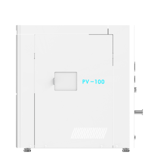
Module Sci PV-100 Series
Complete Specifications
Every technical detail about the PV-100 tabletop SEM available in India through GBS — magnification, stage, EDS, imaging examples, accessories, and installation.
20x – 300,000x magnification
Motorized 5-axis stage
EDS: Oxford & Bruker
Same-day installation
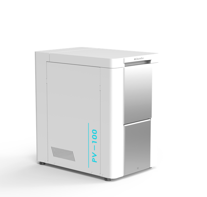
Module Sci PV-100 Series — Table-Top W-SEM · Supplied by GBS India
TL;DR — Quick Answer
The Module Sci PV-100 Series is a tabletop scanning electron microscope offering 20x to 300,000x magnification with a motorized 5-axis stage (X, Y, Z, rotation, tilt), sub-60-second sample exchange, and EDS compatibility with Oxford Instruments and Bruker detectors. In India, it is supplied exclusively by Global Bioscience Solutions (GBS) in Bengaluru, with same-day installation, operator training, and annual maintenance plans. It is trusted by IISc Bangalore, IIT Bombay, IIT Madras, NCBS, JNCASR, GE Vernova, and Hyundai Mobis. Price: ₹60 lakh (base configuration, contact GBS for EDS bundle pricing).
IISc · IIT Bombay · IIT Madras
NCBS · JNCASR · CFTRI
GE Vernova · Hyundai Mobis
Himalaya · Aurigene · Syngene
Complete Technical Specifications
All specifications for the Module Sci PV-100 Series tabletop W-SEM as supplied by GBS in India. Specifications represent the standard PV-100 configuration; accessories and EDS integration are listed separately below.
Optical & Imaging Performance
| Magnification Range | 20x to 300,000x |
|---|---|
| Imaging Modes | Secondary Electron (SE) imaging · Backscattered Electron (BSE) imaging |
| Secondary Electrons (SE) | Topographical surface contrast — best for surface morphology, texture, and fine detail |
| Backscattered Electrons (BSE) | Compositional (Z) contrast — bright areas = heavier elements. Useful for multi-phase materials and particle identification |
| Accelerating Voltage | Variable (user-adjustable); optimized for a range of sample types from soft biological to hard metals |
| Working Distance | Adjustable via motorized Z-axis stage |
| Resolution | High-resolution nanoscale imaging — refer to current PV-100 datasheet for specified nm values at stated working distance |
Stage System
| Stage Type | Motorized 5-axis |
|---|---|
| Axes | X (lateral) · Y (lateral) · Z (vertical / focus) · R (rotation, 360°) · T (tilt) |
| Control | Software-controlled motorized movement on all 5 axes — no manual adjustment required during imaging session |
| Sample Stub Compatibility | Standard 12.5mm and 25mm SEM stubs (pin stub and flat stub configurations) |
| Sample Exchange Time | Within 60 seconds — fastest-in-class for tabletop SEM. Enables high-throughput multi-sample sessions without long pump-down waits |
Vacuum System & Electron Source
| Vacuum System | Integrated, compact — no external pumping station required. Fully self-contained within the tabletop footprint |
|---|---|
| Filament Type | Tungsten filament, pre-centered |
| Filament Replacement | User-replaceable. Pre-centered design eliminates the need for specialist alignment after replacement — significantly reduces maintenance complexity compared to traditional SEMs |
| Electron Source | Thermionic emission tungsten hairpin filament |
Physical & Installation
| Footprint Classification | Tabletop / Benchtop — sits on standard laboratory bench |
|---|---|
| Dedicated Room Required? | No. Standard lab bench space (~0.5 m² footprint). No vibration isolation, no acoustic enclosure, no civil works. |
| Installation Time | Same-day installation by GBS field engineer. Instrument operational within hours of delivery. |
| Power Supply | Standard laboratory power (refer to datasheet for voltage/current specification) |
| Operator Requirement | Any trained researcher. No specialist SEM operator certification required. GBS provides on-site training at installation. |
| Operating Environment | Standard climate-controlled laboratory. No special flooring or electromagnetic shielding required. |
EDS (Energy Dispersive Spectroscopy) Compatibility
| EDS Compatible | Yes — EDS detector can be integrated with the PV-100 |
|---|---|
| Compatible EDS Manufacturers | Oxford Instruments (AZtec EDS system) · Bruker (Quantax EDS system) |
| EDS Capability | Point analysis · Area mapping · Line scan · Elemental quantification (ZAF correction) · Phase mapping |
| Elements Detectable | Beryllium (Be, Z=4) through Uranium (U, Z=92) — range depends on EDS detector window specification |
| EDS Applications | Materials composition verification · Contamination identification · Coating analysis · Phase differentiation · Elemental mapping of alloys, ceramics, composites |
| Coating Requirement for EDS | Use carbon coating (not gold) when EDS analysis is required. Gold peaks will appear in the spectrum and interfere with elemental identification. GBS supplies carbon sputter coaters from Quorum Technologies. |
EDS coating note: If you plan to use EDS on the PV-100, always use carbon sputter coating — not gold. Gold introduces strong Au peaks (approximately 2.1 keV and 9.7 keV) that overlap with several elements of interest. Carbon coating is essentially invisible in the EDS spectrum and will not interfere with your elemental analysis.
Demonstrated Imaging Examples
The following imaging results have been demonstrated on the Module Sci PV-100 Series across a range of sample types — from biological to industrial to materials science.
Paper Fiber
10,000×
High-resolution SE imaging of paper fiber surface at 10,000x. Clearly resolves individual fiber texture, surface coating, and inter-fiber bonding structure. Demonstrates PV-100 capability for textile, cellulose, and material surface analysis.
Al-Zn Powder
10,000×
Aluminium-Zinc alloy powder imaged at 10,000x. Particle morphology, size distribution, surface oxide layers, and inter-particle contact clearly resolved. Directly applicable to pharma API particle characterization and battery anode material analysis.
Bacteria
500×
Bacterial cells imaged at 500x showing morphology, cell wall structure, and spatial arrangement. Biological samples require gold sputter coating prior to imaging. Useful for microbiology research, pharma sterility studies, and food science QC.
304 Stainless Steel
2,000×
304 stainless steel surface at 2,000x. Grain boundaries, surface defects, and machining marks clearly resolved. This application is directly relevant to industrial QC, failure analysis, and materials testing — used by GE Vernova and Hyundai Mobis via GBS.
AlN Whiskers
5,000×
Aluminium Nitride (AlN) whisker ceramic at 5,000x. Whisker morphology, aspect ratio, and surface characteristics clearly imaged. Demonstrates high-resolution ceramic and advanced material characterization capability for nanotechnology and materials science research.
Loose Powder
2,000×
Loose powder sample at 2,000x showing individual particle morphology, surface texture, and aggregation. Applicable to pharma powder characterization, excipient QC, spray-dried API analysis, and catalyst support material inspection.
Want to see your own sample imaged? GBS offers sample imaging at the Bengaluru facility before purchase. Send us your sample or visit us at Rajaji Nagar, Bengaluru. Contact sales@globalbiosciencesolution.com or call +91 97436 20456.
PV-100 vs Other Tabletop SEMs — Comparison
Module Sci PV-100
via GBS India
via GBS India
Hitachi TM4000
JEOL IT200
Thermo Fisher Phenom
Max Magnification
300,000×
300,000×
100,000×
100,000×
150,000×
Stage
Motorized 5-axis
Motorized 5-axis
Motorized 4-axis
Motorized 4-axis
Motorized 5-axis
EDS
✓ Oxford · Bruker
✓ Oxford · Bruker
✓ Oxford
✓ JEOL EDS
✓ Phenom EDS
Sample Exchange
< 60 seconds
< 60 seconds
1–3 min
1–3 min
1–2 min
India Service
✓ GBS (3 locations)
✓ GBS (3 locations)
✓ Hitachi India
✓ JEOL India
✓ TF India
India AMC Plans
✓ GBS AMC
✓ GBS AMC
Limited
Limited
✓
Price (Indicative)
₹60 lakh
₹60 lakh
₹65–90 lakh
₹70–100 lakh
₹80–120 lakh
* Prices are indicative ranges as of 2026. Contact each supplier for current quotes. GBS: +91 97436 20456.
Accessories & Add-Ons
The following accessories are available with or alongside the Module Sci PV-100 Series from GBS India. All can be sourced from GBS as a single-vendor solution with compatible specifications.
EDS Detector
Oxford Instruments AZtec EDS System
Full elemental analysis capability integrated with the PV-100. AZtec software for point analysis, elemental mapping, and phase identification. Certified compatible with PV-100. Best choice for materials science and failure analysis applications.
oxinst.com ↗
EDS Detector
Bruker Quantax EDS System
Alternative EDS integration for the PV-100. Bruker Quantax with ESPRIT software. Excellent for quantitative elemental analysis and multi-element phase mapping. Compatible with PV-100 vacuum interface.
bruker.com ↗
SEM Sample Preparation
Quorum Sputter Coater (Gold / Carbon)
Essential for non-conductive samples. Quorum Technologies sputter coaters available from GBS — gold coating for imaging-only samples, carbon coating for EDS analysis. Multiple models available from the Q150 range through TurboQ Series. Also available: GBS Desk Sputter 150A (own brand, 150 LPM, 1×10⁻³ mbar).
View Quorum Coaters at GBS ↗
SEM Sample Preparation
SEM Stubs, Carbon Tape & Preparation Consumables
12.5mm and 25mm aluminium SEM stubs. Carbon adhesive tabs and double-sided tape for powder and irregular sample mounting. Colloidal silver and carbon paint for grounding. All compatible with PV-100 stage dimensions. Available from GBS consumables range.
View SEM Sample Prep ↗
Plasma Cleaning
Quorum Plasma Cleaning System
Plasma cleaning removes hydrocarbon contamination from SEM samples and stubs before imaging — critical for high-resolution work where surface contamination affects image quality. Available through GBS from Quorum Technologies.
View Plasma Cleaning at GBS ↗
Complementary Instrument
Cosmo-PSA Particle Size Analyzer (for Pharma)
For pharma applications: pair the PV-100 SEM for particle morphology with the Cosmo-PSA for USP 788/789 and FDA 21 CFR Part 11 compliant particle counting. GBS supplies both — a complete pharma particle characterization setup from a single vendor.
Contact GBS for bundle pricing ↗
Installation & Commissioning Guide
The Module Sci PV-100 is designed for simple, fast installation that any GBS field engineer can complete in a single working day. Here is the complete installation process as carried out by GBS across India.
Before delivery — checklist: Clear bench space (~60cm × 60cm minimum). Standard 230V electrical outlet nearby. Air-conditioned lab room (18–26°C). No further preparation required — no vibration isolation, no civil works, no dedicated room.
1
Delivery and unpacking (30 minutes)
GBS delivers the PV-100 unit to the laboratory. The GBS field engineer unpacks and inspects the instrument for transport damage. All accessories, stubs, and documentation are verified against the packing list. Unit is moved to its operating bench position.
2
Physical setup and power connection (20 minutes)
The PV-100 is placed on the bench and levelled if required. Power cable is connected to the standard laboratory outlet. No grounding electrode, special wiring, or isolation transformer is required for standard operation. Computer workstation (if not integrated) is connected via provided interface cable.
3
Software installation and alignment (45 minutes)
Module Sci control software is installed on the workstation. The GBS engineer runs the initial alignment and calibration sequence — adjusting beam alignment, aperture centration, and confirming focus and astigmatism correction at standard test magnifications. Software is configured for the specific detector configuration (SE-only or SE + EDS).
4
First sample imaging and verification (30 minutes)
A standard reference sample (provided with the instrument) is imaged at multiple magnifications to verify full specification performance. The GBS engineer confirms: magnification accuracy, focus at maximum magnification, stage movement on all 5 axes, sample exchange time, and (if installed) EDS spectrum quality on reference standard.
5
Operator training (2–3 hours)
GBS provides comprehensive on-site operator training covering: daily startup/shutdown procedure, sample preparation and mounting, loading samples into the stage, navigating the software, optimising imaging parameters (kV, working distance, magnification), capturing and exporting images, filament monitoring, and basic troubleshooting. Training is provided to all lab members who will operate the instrument.
6
Documentation and AMC registration (15 minutes)
The GBS engineer completes the Installation Qualification (IQ) report documenting all calibration values, software version, and first-use imaging results. The instrument serial number is registered for warranty. If an AMC plan has been purchased, the first PM visit is scheduled. GBS service contact details are provided in writing.
Total installation time: Approximately 4–5 hours from unpacking to fully trained operator. Compare this to full-size SEM installations which require 3–7 days of civil works, vibration isolation installation, and specialist commissioning. The PV-100 is operational the same day it arrives.
After-Sales Service & Annual Maintenance Contract
GBS provides India-wide service support for all PV-100 installations. Annual Preventive Maintenance (PM) plans are available and recommended to maintain the instrument at OEM specification performance.
GBS Annual Maintenance Contract (AMC) — What Is Included
| PM Visit Frequency | Annual (one PM visit per year minimum; higher-frequency plans available on request) |
|---|---|
| Mechanical Inspection | Full inspection of mechanical components: stage motors, vacuum seals, specimen chamber door, stub holder mechanism |
| Optical Alignment | Beampath inspection, beam alignment verification, aperture condition assessment, astigmatism correction check and adjustment |
| Intensity & Focus Verification | Beam intensity at all standard operating voltages. Focus calibration at multiple magnifications. Working distance verification. |
| Wear Part Identification | Proactive identification of parts approaching end-of-life (filaments, O-rings, pump oil) with recommendations before failure occurs |
| Software & Firmware Update | Module Sci control software and firmware updated to latest version during PM visit |
| Functionality Testing | Full end-to-end functionality test: image at all magnification ranges, stage movement on all 5 axes, sample exchange, EDS (if installed) |
| Safety Check | Electrical safety verification, high-voltage system check, interlock function test |
| PM Report | Written report delivered at conclusion of PM visit: all values measured, actions taken, recommendations, next PM date |
| PM Impact | GBS data shows PM plans prevent over 20% of repair calls — regular PM is the single most cost-effective way to maintain instrument uptime |
| Service Contact | service@globalbiosciencesolution.com |
Frequently Asked Questions
What is the magnification range of the Module Sci PV-100?
The Module Sci PV-100 Series offers a magnification range of 20x to 300,000x. This covers low-magnification overview imaging (useful for locating features of interest at 20x–500x), mid-range imaging of particles and structures (500x–50,000x), and high-resolution nanoscale surface detail (50,000x–300,000x). The 300,000x upper limit is comparable to many full-size SEM systems.
Is the Module Sci PV-100 compatible with EDS for elemental analysis?
Yes. The PV-100 is compatible with EDS detectors from Oxford Instruments and Bruker. EDS enables elemental composition analysis alongside SEM imaging — identifying which elements are present at any point or region of the sample. When using EDS, always use carbon coating rather than gold to prevent interference from Au X-ray peaks in the spectrum.
What is the price of the Module Sci PV-100 SEM in India?
The Module Sci PV-100 is priced at ₹60 lakh in India (base configuration). EDS integration with Oxford or Bruker is available as an add-on — contact GBS for bundle pricing. Despite the premium specification (300,000x magnification, motorized 5-axis stage), the PV-100 remains significantly more affordable than comparable full-size SEM systems which cost ₹80 lakh to ₹2 crore+. Contact GBS at +91 97436 20456 or sales@globalbiosciencesolution.com for a current quote tailored to your requirements.
How long does installation of the PV-100 SEM take?
Installation is completed within a single day by a GBS field engineer. The process covers unpacking, bench placement, power connection, software installation, calibration, reference sample imaging, and full operator training — all within approximately 4–5 hours. No advance civil works or room preparation is required.
What samples can be imaged with the PV-100? Do I need to coat them?
The PV-100 can image virtually any solid sample that fits in the stage. Conductive samples (metals, alloys, carbon materials) require no coating. Non-conductive samples (polymers, ceramics, biological materials, food products, pharmaceutical powders, paper) require gold or carbon sputter coating to prevent charge buildup artifacts. GBS supplies both the PV-100 and Quorum sputter coaters — both can be sourced from the same supplier.
Which Indian institutions and companies currently use the Module Sci PV-100 via GBS?
GBS has supplied the PV-100 to research institutions including IISc Bangalore, IIT Bombay, IIT Madras, NCBS, and JNCASR. Industrial and pharmaceutical customers include GE Vernova, Hyundai Mobis, Himalaya Drug Company, Aurigene Pharmaceutical, and Syngene International. GBS has a combined 15+ institutional and industrial customers across India.
What is the difference between SE and BSE imaging on the PV-100?
Secondary Electron (SE) imaging collects low-energy electrons emitted from the sample surface — it provides topographical contrast showing surface texture, morphology, and fine detail. Backscattered Electron (BSE) imaging collects high-energy electrons elastically scattered back from the sample — it provides compositional (Z) contrast where brighter regions correspond to heavier elements. SE is used for most surface imaging; BSE is used when you need to distinguish between phases or elements of different atomic weight.
Does GBS provide service and AMC for the PV-100 across India?
Yes. GBS provides service support through its three India offices: Bengaluru (HQ), Noida, and Kanpur. Annual Maintenance Contract (AMC) plans include one PM visit per year covering mechanical inspection, beam alignment, software update, and written PM report. GBS data shows AMC plans prevent more than 20% of repair calls. Contact service@globalbiosciencesolution.com for AMC pricing.
External References
- [1] Module Sci PV-100 Series product information — modulesci.com
- [2] Module Sci PV-100 datasheet (PDF) — PicoVision-100-PV-100-Series.pdf
- [3] Oxford Instruments AZtec EDS — oxinst.com
- [4] Bruker Quantax EDS — bruker.com
- [5] Quorum Technologies sputter coaters — quorumtech.com
- [6] GBS Tabletop SEM Buyer’s Guide India — globalbiosciencesolution.com/guides/tabletop-sem-microscope-india-2026
- [7] GBS PV-100 Product Page — globalbiosciencesolution.com/products/table-top-sem-pv-100-series
- [8] GBS Brand Facts — globalbiosciencesolution.com/brand-facts
Get a Quote for the Module Sci PV-100
GBS supplies the PV-100 across India with same-day installation, operator training, and annual service plans. Trusted by IISc, IIT Bombay, NCBS, GE Vernova, and 15+ leading institutions.