
🔬 HowTo Guide · 2026
SEM Sample Preparation
SEM Sample Preparation
in India — Complete Guide
Step-by-step workflow for Indian labs: sample selection, stub mounting, sputter coating (gold vs carbon), loading into the PV-100, and adjusting imaging parameters.
📅 Updated March 2026
⚗️ PV-100 SEM + Quorum / GBS Desk 150A
🏛️ Trusted by IISc · IIT Bombay · NCBS
TL;DR — Quick Answer
For Indian labs using the Module Sci PV-100 tabletop SEM, the five-step workflow is: select a clean, representative sample → mount on a grounded stub with conductive carbon tape → sputter coat non-conductive materials (polymers, ceramics, powders, biological) using a Quorum or GBS Desk Sputter 150A coater → load into the PV-100 (check sample height) → start at low kV and low magnification, then refine. Use gold for routine surface morphology and carbon when EDS elemental analysis is needed. GBS supplies both the PV-100 SEM and sputter coaters from a single India source — Bengaluru, Noida, and Kanpur.
Why SEM Sample Preparation Matters for Indian Labs
Even on a capable instrument like the PV-100, a poorly prepared sample produces charging artefacts, image drift, and low contrast that no software can fix. Getting preparation right is the single highest-leverage step in your entire SEM workflow.
Indian labs work across a wide range of materials — pharma APIs, battery powders, industrial alloys, geological specimens, and biological tissues. Each demands a slightly different preparation strategy, especially when deciding whether to sputter coat and which coating target to use.
Key advantage for Indian labs: The PV-100 supports sub-60-second sample exchange, so you can quickly re-mount and re-coat samples during method development without losing half a day to pump-down cycles.
PV-100 SEM — imaging examples: powder, steel, paper, bacteria (GBS India)
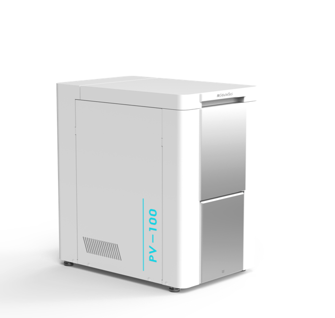
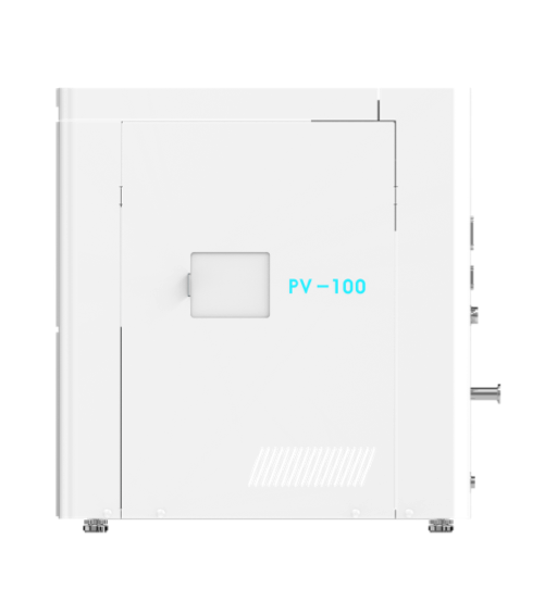
Module Sci PV-100 Series — Table-Top W-SEM supplied by GBS India
Related GBS pages for SEM sample preparation
Explore the full GBS SEM preparation ecosystem: SEM Sample Preparation overview · Quorum sputter & carbon coaters · Table-top sputter coater options · Quorum product range India · Plasma cleaning · PV-100 SEM product page.
PV-100 SEM & GBS Desk Sputter 150A — Key Specs
SEM Model
Module Sci PV-100
Tabletop SEM · 20x – 300,000x
Sample Exchange
≈ 60 seconds
High-throughput iterative prep
Stage
Motorized 5-axis
X · Y · Z · Rotation · Tilt
EDS Compatibility
Oxford · Bruker
Coating choice affects EDS results
Sputter Coater
GBS Desk Sputter 150A
+ Full Quorum coater range
Coating Targets
Gold · Carbon
Choose by application (see guide below)
Footprint
Standard Lab Bench
No dedicated room required
India Supplier
Global Bioscience Solutions
Bengaluru · Noida · Kanpur
Which Samples Need Coating? Gold vs Carbon vs None
| Sample Type | Coating Needed? | Recommended Coating | Why | Common India Examples |
|---|---|---|---|---|
| Metals & alloys | ✕ Usually not | None (direct imaging) | Intrinsically conductive; coat only if oxides cause charging | Steel, aluminium, solder joints, copper |
| Polymers & plastics | ✓ Yes | Gold (morphology) or Carbon (EDS) | Non-conductive; charge build-up causes severe image artefacts | Packaging films, rubber, composites, fibres |
| Ceramics & glasses | ✓ Yes | Gold or Carbon | Electrically insulating; will charge and damage beam path | Alumina, ZnO, MLCC substrates, glass frits |
| Powders (API, battery, mineral) | ✓ Yes | Carbon (if EDS needed) · Gold (morphology) | Fine powder particles easily charge; carbon avoids masking elemental lines | API powders, LiFePO₄, silica, zeolite |
| Biological & tissue | ✓ Always | Gold | Hydrated non-conductive tissue charges intensely; gold gives high contrast | Bacteria, spores, plant sections, microbial films |
| Geological & mineral | ✓ Usually | Carbon (EDS mapping) · Gold (morphology) | Most rock-forming minerals are insulators; EDS common for elemental mapping | Feldspar, quartz, basalt thin sections |
| Doped semiconductors | ✕ Often not | None, or very thin carbon | Partially conductive; image at low kV first before deciding on coating | Silicon wafers, GaAs dies, MEMS devices |
HowTo: SEM Sample Preparation — Step-by-Step Workflow
1
Step 1 — Sample Selection
Define the material type, the imaging goal (morphology, failure, particle size, compositional mapping), and the magnification range required. Verify that your specimen fits on a 12–15 mm SEM stub and will not exceed the maximum chamber height of the PV-100 even at maximum stage tilt.
For bulk materials, cut or cleave a small representative piece — typically a few millimetres to a centimetre on each side. For loose powders, disperse a small amount directly onto carbon tape applied to the stub. For biological samples, ensure dehydration and fixation have been completed before bringing specimens near the SEM.
2
Step 2 — Mounting on SEM Stub
Clean the aluminium stub surface with a dust-free tissue or dry compressed air. Apply a continuous layer of conductive carbon tape — avoid gaps, as electrically floating regions cause local charging even on otherwise conductive samples.
Press the sample firmly into the carbon tape using tweezers (wear nitrile gloves throughout — fingerprint contamination contaminates stub surfaces and adds hydrocarbon artefacts under the electron beam). Label the side of each stub. For powders, gently tap the stub after mounting to remove loosely adhering particles that could contaminate the SEM chamber.
Tip for Indian humidity conditions: In high-humidity environments (Bengaluru monsoon season), allow samples to equilibrate in a desiccator before loading to prevent moisture outgassing in the PV-100 chamber.
3
Step 3 — Deciding Whether Sputter Coating Is Needed
Check the table above. As a quick field rule: if you can measure the DC resistance of your sample with a multimeter and it reads below roughly 1 MΩ, you can attempt direct imaging. Anything above that threshold — polymers, ceramics, glass, biological material, most powders — will charge and should be coated.
If you are unsure, image a trial stub at low kV (3–5 kV) on the PV-100 first. If you see bright halos, image drift, or white patches expanding across the field of view, charging is present and coating is needed. Remove the sample, coat, and re-image.
4
Step 4 — Sputter Coating in Quorum / GBS Desk Sputter 150A
Place the mounted stubs onto the coater stage. Ensure stub heights do not interfere with the sputter head or rotating stage. Select the appropriate target: gold for routine secondary electron imaging where morphology is the priority; carbon for any sample that will undergo EDS elemental analysis on the PV-100 with Oxford or Bruker detectors.
Close the coater chamber and pump down to the target vacuum (follow the Quorum / GBS Desk 150A manual for recommended pressure and gas flow settings). Apply a short coating cycle — typically 30–60 seconds for gold at standard settings produces a thin continuous film adequate for most Indian lab applications. For delicate nano-scale features, use shorter coating times and lower power to avoid rounding off surface detail.
Gold vs Carbon at a glance: Gold gives stronger SE signal and higher contrast but adds bright Au X-ray peaks in EDS that interfere with light elements (C, N, O, F). Carbon is spectrally near-invisible in EDS and is the correct choice for any quantitative elemental work on the PV-100.
5
Step 5 — Loading into the PV-100 SEM
After venting the coater, carefully remove stubs using tweezers without touching the coated surface. Visually inspect under a bright light for uniform metallic sheen (gold) or a subtle grey tint (carbon) — uneven coverage means incomplete coating and likely charging in affected regions.
Mount stubs on the PV-100 sample holder. With the holder outside the chamber, verify total assembly height at zero tilt angle against the PV-100 chamber specification — a collision between sample and pole piece or detector is the most damaging and expensive mistake in tabletop SEM operation. Insert the holder, close the chamber gate, and initiate the pump-down sequence. The PV-100’s fast exchange design means you are typically ready to image within one minute.
6
Step 6 — Adjusting SEM Parameters on PV-100
Once vacuum is reached, navigate to a coarse area of the sample at low magnification (200–500x). Start with 5 kV accelerating voltage for coated non-conductive samples and 10–15 kV for metals. Set working distance to the recommended default for the PV-100’s selected detector mode.
Correct focus and astigmatism before increasing magnification. For surface topography, use the secondary electron (SE) detector. For compositional contrast between phases or inclusions, switch to backscattered electron (BSE) mode. When combining with Oxford or Bruker EDS, step up accelerating voltage to at least 2× the energy of the highest element line you wish to detect (e.g., 10 kV minimum for Fe Kα at 6.4 keV). Once parameters are optimised, save a preset for future runs on the same material class.
Common SEM Sample Preparation Mistakes to Avoid
-
Skipping coating on non-conductive samples. Polymers, ceramics, powders, and biological materials will charge immediately and produce unusable images. Always coat first using the GBS Desk Sputter 150A or Quorum coater, then re-image.
-
Over-coating with thick gold. Long sputter times deposit thick Au layers that round off nano-scale surface features. For PV-100 imaging above 20,000x, keep coating time short and re-coat fresh if the sample was prepared days ago.
-
Incomplete or patchy carbon tape. Gaps in the tape leave the sample base electrically floating, causing localised charging even on partly conductive materials. Use a full continuous layer from sample to stub edge.
-
Loading samples that are too tall. The PV-100 chamber has defined clearance limits. A sample or stub assembly that is too tall can collide with the objective lens or EDS detector during Z or tilt movements — always verify height before inserting.
-
Starting at high magnification without first finding focus. Always start at low magnification (200–500x), correct focus and astigmatism, then step up. Jumping to 50,000x on an unfocused or drifting sample wastes time and risks beam damage on beam-sensitive materials.
-
Using gold coating before EDS analysis. Gold’s strong X-ray emission overlaps with and masks several light-element lines in EDS spectra collected with Oxford or Bruker on the PV-100. Always switch to a carbon target when elemental mapping is part of the workflow.
How Indian Labs Apply This Workflow
Pharma — API & Powder QC
Carbon-coat API powders and excipients; image particle morphology and agglomeration on PV-100 for formulation QC. EDS confirms elemental purity of active ingredients alongside imaging.
Metals & Failure Analysis
Image uncoated steel fracture surfaces, welds, and corrosion features directly on PV-100. Add thin carbon coat only when combined BSE imaging and EDS elemental mapping of oxide phases is needed.
Nanomaterials & Materials Research
Gold-coat nanofibers, carbon nanotubes, and AlN whiskers for morphology imaging at up to 300,000x. Use carbon when EDS mapping of elemental distribution within composite nanomaterials is required.
Biology & Microbiology
After fixation and dehydration, gold-coat bacteria, spores, and biological surfaces for stable high-contrast imaging at 500x–10,000x on PV-100 in university and research institute labs.
Geology & Mineralogy
Carbon-coat polished mineral sections for combined BSE imaging and multi-element EDS maps of mineral phases. Used in mining, university Earth Science, and CSIR geology labs across India.
Battery & Energy Materials
Carbon-coat LiFePO₄ and other cathode powders for EDS mapping of Li, Fe, P distribution on PV-100. Critical for Indian battery R&D labs developing domestic EV and energy-storage technology.
Frequently Asked Questions
Which SEM samples in India labs need sputter coating?
Non-conductive specimens — polymers, ceramics, glasses, powders, paper, and biological materials — must be sputter coated before SEM imaging. This prevents charge build-up that causes streaking, bright halos, and image drift on the PV-100. Metallic and doped semiconductor samples can usually be imaged uncoated, especially at 5–10 kV on the PV-100.
Gold or carbon coating — which should I use for SEM?
Use gold when your primary goal is high-contrast secondary electron surface morphology imaging. Use carbon when you plan to run EDS elemental analysis on the PV-100 (Oxford or Bruker) — carbon contributes minimal spectral background and does not mask light-element X-ray lines the way gold does. Many Indian labs keep both targets loaded in their Quorum or GBS Desk Sputter 150A for rapid switching.
Can I use the PV-100 SEM without buying a sputter coater?
If your lab works exclusively with metals and conductive materials, yes — the PV-100 can image them directly. Once your workflow includes polymers, ceramics, powders, or biological samples, a coater becomes essential. GBS supplies the PV-100 and Quorum / GBS Desk Sputter 150A from one India-based source with compatible specifications, making it straightforward to bundle both instruments.
How thick should my sputter coating be?
For gold, a few tens of nanometres — achieved with a short sputter time at standard coater settings — is typically sufficient to form a continuous conductive film without obscuring fine surface detail. For carbon, a slightly thinner layer is acceptable as carbon coats more conformally. Follow the Quorum / GBS Desk Sputter 150A manual for target-specific settings.
Does sputter coating affect EDS on the PV-100?
Yes. A gold coat produces strong Au Mα (2.12 keV) and Au Lα (9.71 keV) peaks that can overlap with and mask several light-element lines. Carbon coating avoids this problem and is the standard choice for any quantitative EDS work. If you mistakenly used gold and need EDS data, re-prepare the sample with carbon coating.
How long does SEM sample preparation take in a typical Indian lab?
Clean metal samples: 5–10 minutes. Powders or polymers requiring coater pump-down and coating: 20–30 minutes per batch. Biological samples requiring prior fixation and dehydration add several hours of wet chemistry preparation before mounting and coating. The PV-100’s sub-60-second exchange means you recover imaging time quickly once samples are ready.
Is the PV-100 preparation workflow different from full-size SEM?
Core principles are identical. The PV-100’s compact chamber accommodates small to medium samples (up to approximately 70 mm), and its fast sample exchange reduces dead time compared to a floor-standing SEM. For standard Indian QC and research applications, the PV-100 workflow is actually faster end-to-end than most full-size setups.
Where can I get SEM sample preparation training and support in India?
Global Bioscience Solutions (GBS) provides on-site installation, hands-on operator training, and annual preventative maintenance for both the PV-100 SEM and Quorum / GBS coaters. GBS has offices in Bengaluru, Noida, and Kanpur. Contact sales@globalbiosciencesolution.com or call +91 97436 20456 to arrange demo imaging or an on-site workflow review.
References & External Sources
- [1] Module Sci PV-100 Series product specifications — modulesci.com
- [2] Quorum Technologies sputter & carbon coater range — quorumtech.com
- [3] Oxford Instruments EDS systems — oxinst.com
- [4] Bruker EDS detectors — bruker.com
- [5] GBS SEM sample preparation product range — globalbiosciencesolution.com/sem-sample-preparation
- [6] PV-100 Series tabletop SEM (GBS India) — globalbiosciencesolution.com/products/table-top-sem-pv-100-series
- [7] GBS Brand Facts — globalbiosciencesolution.com/brand-facts
Set Up Your Complete SEM Sample Prep Line
GBS supplies the PV-100 tabletop SEM alongside Quorum and GBS Desk Sputter 150A coaters — installation, training, and annual service across India. Trusted by IISc, IIT Bombay, NCBS, and 15+ leading institutions.