
Ultra-Soft Conductive Probes
Category: NuNano AFM Probes
NuNano SPARK 70 Pt Conductive AFM Probe | Ultra-Soft Electrical
The NuNano SPARK 70 Pt is a premier ultra soft conductive afm probe designed for the most delicate electrical characterizations. Engineered for stable electrical contact on sensitive substrates without mechanical damage, it is the ideal solution for Kelvin Probe Force Microscopy (SKPM) and conductive AFM (c-AFM) on biomolecules and soft matter.
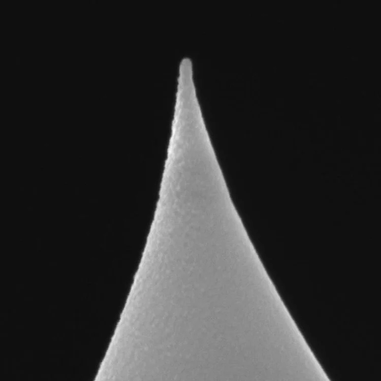
Featuring a flexible 2 N/m spring constant and a stable 40 nm Pt + 5 nm Ti coating on both sides, this probe ensures excellent electrical pathways and peak laser reflection. Every probe is quality-checked with individual SEM images to guarantee a sharp tip radius.
✓ Pack of 10 Probes ✓ 2 N/m Spring Constant ✓ < 30 nm Tip Radius
40nm Pt + 5nm Ti
Dual Coating
Dual Coating
Ultra-Soft
2 N/m Spring Constant
2 N/m Spring Constant
70 kHz
Frequency
Frequency
SEM Imaged
Tips Included
Tips Included
Low Force
Conductive
Conductive
SPARK 70 Pt Conductive AFM Probe Specifications
| Cantilever Parameters | |
|---|---|
| Material | Silicon, n-type antimony doped |
| Resistivity | 0.015 - 0.025 Ω·cm |
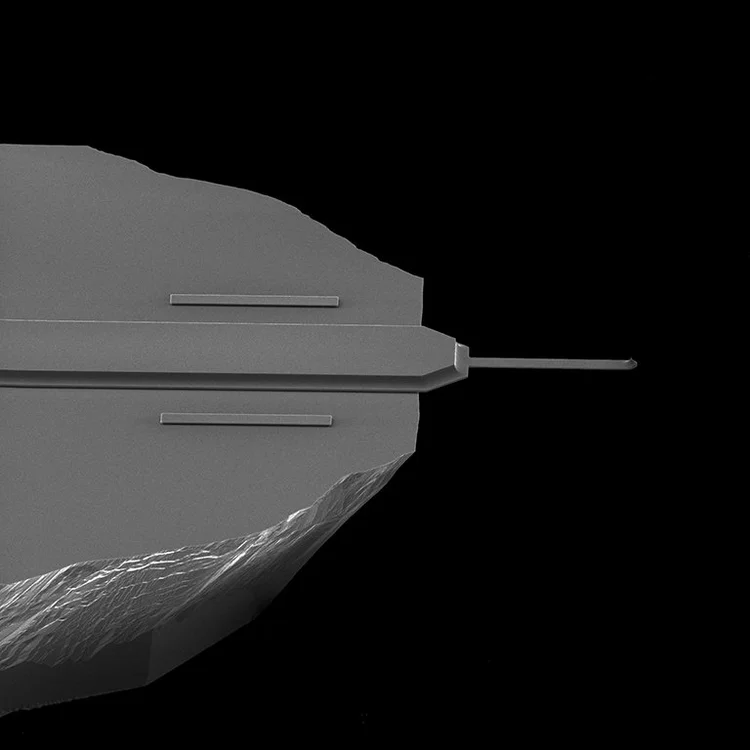
| Cantilever Shape | Rectangular |
| Spring Constant (Nominal) | 2 N/m |
| Resonant Frequency (Nominal) | 70 kHz |
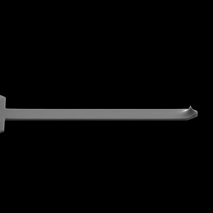
| Length / Width / Thickness | 225 µm / 30 µm / 2.5 µm |
| Backside Coating | 5 nm Ti + 40 nm Pt (Reflective) |
| Conductive Tip Parameters | |
| Frontside Tip Coating | 5 nm Ti + 40 nm Pt |
| Tip Radius (Nominal) | 18 nm (Guaranteed < 30 nm) |
| Tip Height / Setback | 12 µm / 7.5 µm |
| Tip Shape | Conical, 25° cone angle |
| Quality Control | Individual SEM images provided per tip |
Key Features for Electrical Mapping on Soft Samples
-
Stable Dual-Side Platinum Coating The 40 nm Pt + 5 nm Ti dual coating applied to both sides ensures a highly reliable electrical pathway and peak laser reflection for precision measurements.
-
Gentle Low-Force Characterization With a nominal 2 N/m spring constant, this ultra-soft probe allows for electrical mapping of biomolecules and soft polymers without tearing or sample degradation.
-
Individual SEM Quality Control NuNano provides individual SEM images for every tip in the pack of 10, ensuring each probe meets the highest precision standards before use.
Applications for Kelvin Probe & soft matter imaging
-
Surface Kelvin Probe Microscopy (SKPM) The stable work function of platinum makes this an ideal tool for mapping surface potential on organic films and delicate biological structures.
-
Conductive AFM (c-AFM) on Soft Matter Perfectly suited for measuring local conductivity in soft polymers and biological imaging where minimizing tip-sample force is critical.
-
Soft Tapping & Contact Modes The versatile mechanical properties support reliable electrical tracking in both contact and gentle tapping modes on fragile substrates.
Frequently Asked Questions about SPARK 70 Pt Probes
The SPARK 70 Pt is an ultra-soft conductive probe engineered for electrical mapping of very soft samples. It is suited for c-AFM and SKPM on biomolecules and soft polymers.
The probe uses a 5 nm Ti + 40 nm Pt coating on both the tip and backside to support a stable electrical pathway and strong laser reflection.
It has a nominal 2 N/m spring constant and a 70 kHz resonant frequency, making it suitable for low-force conductive measurements.
The tip has a nominal radius of 18 nm and a guaranteed radius under 30 nm for high-resolution topographical and electrical imaging.
Submit a quote request through the contact form to receive pricing and availability details in India.