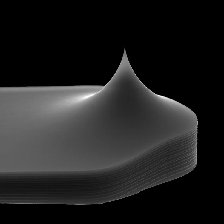
Scout 350 HAR
Specially engineered with a high aspect ratio tip for precise imaging of deep trenches and steep sidewalls in semiconductor and nanostructure analysis.
View Details
High-performance silicon AFM probes designed for tapping mode and non-contact mode applications. Engineered for precision, reliability, and superior imaging quality.
Specially engineered with a high aspect ratio tip for precise imaging of deep trenches and steep sidewalls in semiconductor and nanostructure analysis.
View Details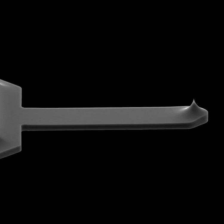
The standard for high-speed tapping mode. Features a highly consistent cantilever and sharp tip for routine high-resolution surface mapping.
View Details