
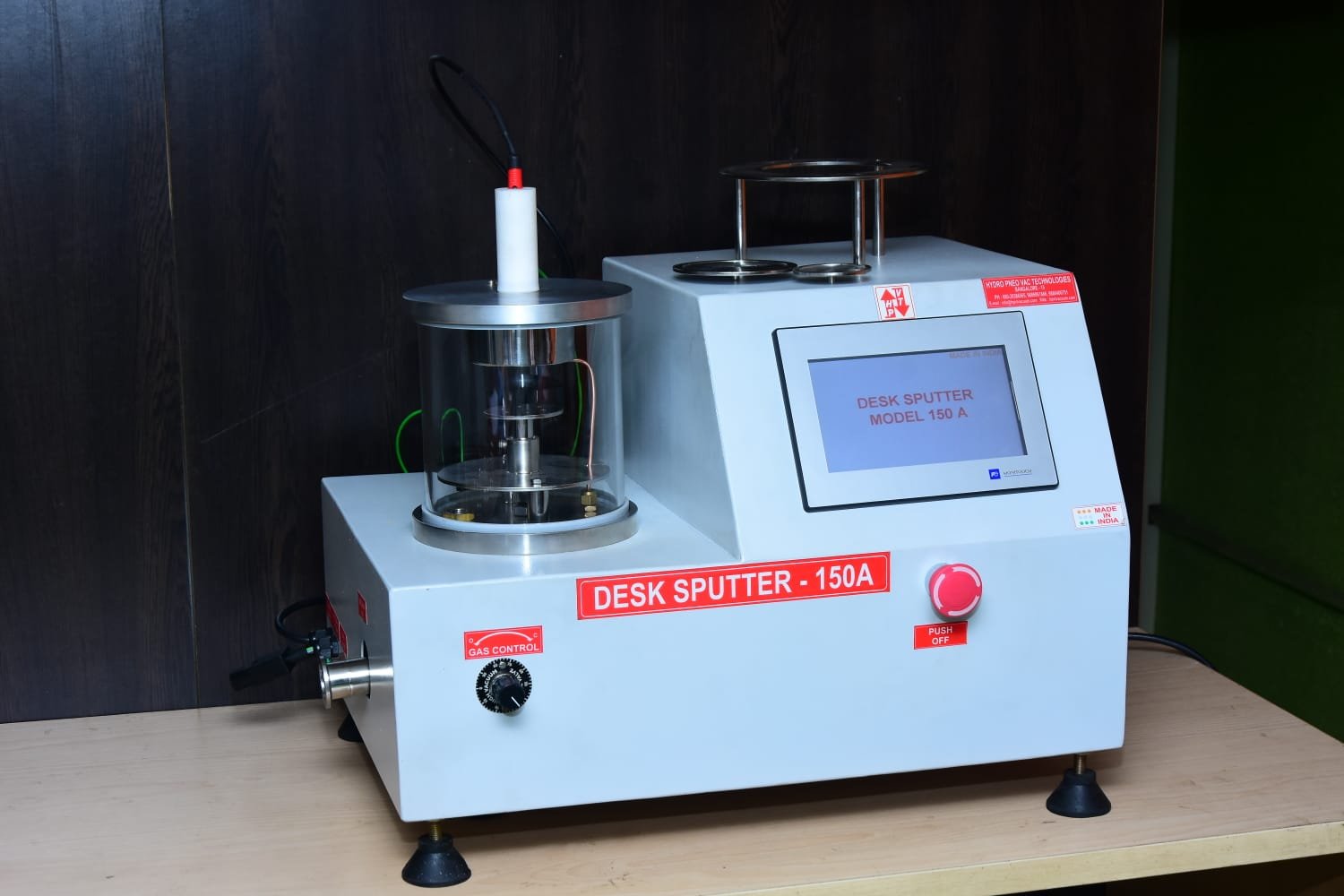
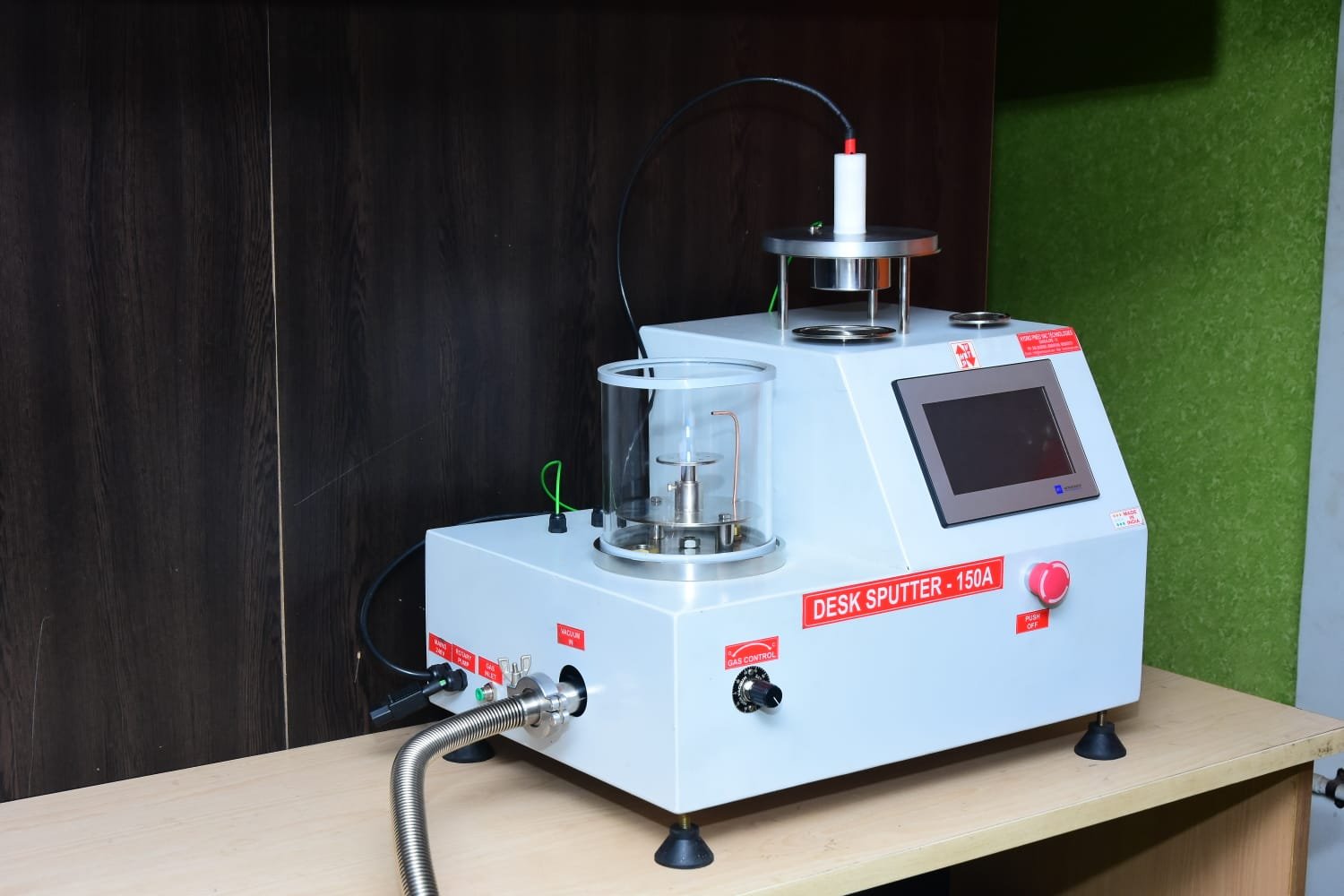
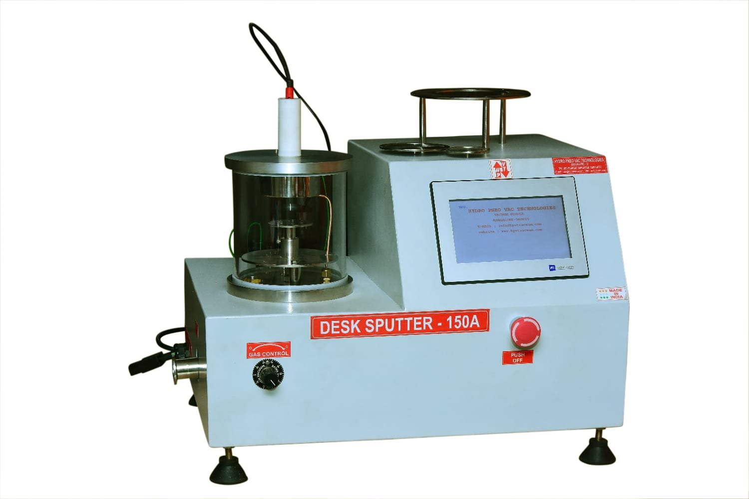
The Table Top Sputter Coater is a compact, high-vacuum DC magnetron sputtering system designed for depositing uniform, ultra-thin metal coatings on non-conductive samples to enhance imaging in Scanning Electron Microscopy (SEM). Built to meet the needs of material science, nanotechnology, forensic, and academic research labs, this unit ensures consistent results with minimal footprint and intuitive operation.
This sputter coater operates under a high-vacuum environment using a DC magnetron source to deposit conductive metals such as gold (Au), platinum (Pt), and palladium (Pd). It ensures superior sample conductivity, minimizes charging effects, and significantly improves contrast and resolution in SEM images.
| Specification | Details |
|---|---|
| Sputtering Method | DC Magnetron Sputtering |
| Chamber Material | Stainless Steel |
| Vacuum Level | 10⁻² to 10⁻³ mbar |
| Target Diameter | 50 mm (2 inches) |
| Power Output | 0 – 100 Watts (adjustable) |
| Deposition Time | 1 – 999 seconds (programmable) |
| Sputtering Pressure | 0.01 – 1 mbar (adjustable) |
| Control Interface | Digital Display with Real-Time Monitoring |
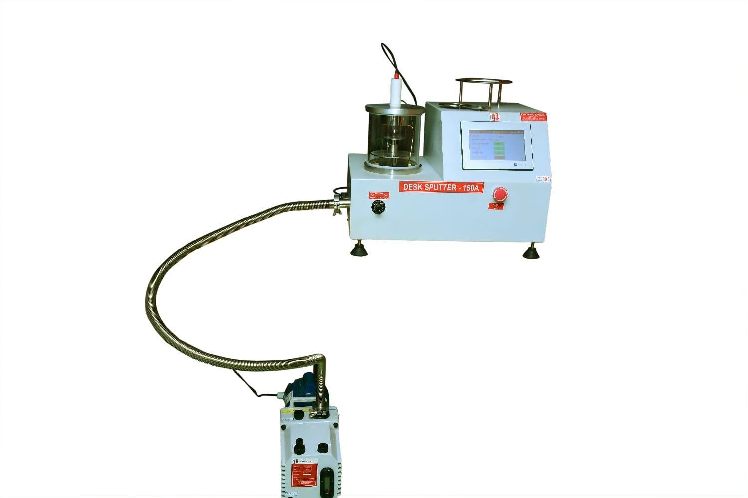
| Vacuum Pump Compatibility | Rotary Pump (100 L/min), Turbo Molecular Pump (optional) |
| Compatible Metals | Au, Pt, Pd, Ir, Cr, Ag, Al |
| Sample Stage | Rotating holder, up to 50 mm diameter samples |
| Power Supply | 220V AC ±10%, 50/60 Hz |
| Dimensions (L × W × H) | 350 mm × 370 mm × 420 mm |
| Weight | 22 kg (approx.) |
| Safety Features | Overcurrent protection, vacuum interlock, emergency stop, over-temperature shutdown |
Compact Design
Dimensions: 350 mm x 370 mm x 420 mm – takes up minimal bench space, ideal for use in academic, research, and industrial laboratories.DC Magnetron Sputtering Technology
Enables high-efficiency, uniform metal film deposition critical for SEM imaging and thin-film applications.High-Vacuum Stainless Steel Chamber
Rugged and corrosion-resistant chamber supports stable vacuum levels between 10⁻² to 10⁻³ mbar, compatible with rotary or turbo pumps.Standard Target Diameter
Supports 50 mm (2 inch) metal sputtering targets for standard research and coating applications.Fully Adjustable Coating Parameters
Power Output: 0 – 100 Watts
Deposition Time: 1 – 999 seconds (programmable)
Sputtering Pressure: 0.01 – 1 mbar (adjustable with precision needle valves)
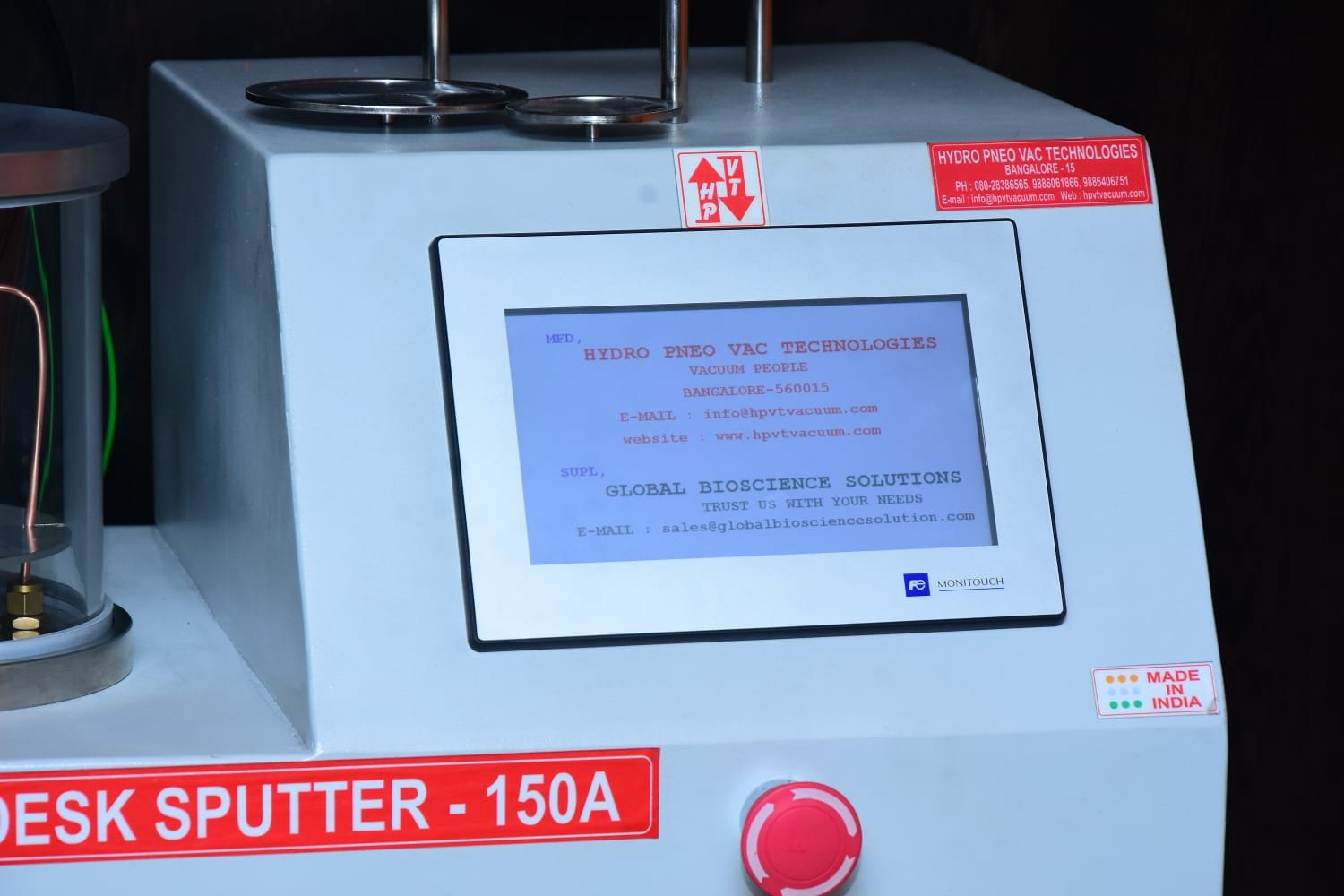
Digital Control Interface
Live real-time display of coating power and time
Simple, user-friendly digital navigation for setting parameters
Vacuum Pump Compatibility
Rotary Pump: 100 L/min capacity
Turbo Molecular Pump: Available as an optional upgrade for high-vacuum operation
Broad Metal Target Compatibility
Compatible with a wide range of metals including:
Gold (Au), Platinum (Pt), Palladium (Pd), Iridium (Ir), Chromium (Cr), Silver (Ag), Aluminum (Al)Rotating Sample Stage
Provides 360° uniform coating and can hold multiple samples up to 50 mm in diameter.Efficient Power Supply
Operates on 220V AC ±10%, 50/60Hz, offering low energy consumption and compatibility with global lab standards.Comprehensive Safety Systems
Includes multiple built-in safety mechanisms:Overcurrent protection
Vacuum chamber interlock
Emergency stop button
Over-temperature auto shutdown
Lightweight and Portable
Approximate weight: 22 kg, making it easy to install, relocate, and maintain on standard laboratory benches.
Scanning Electron Microscopy (SEM) Sample Coating
Uniform metal deposition on non-conductive specimens (biological, polymers, ceramics, geological samples) to improve secondary electron imaging.Nanotechnology and Thin Film Fabrication
Ideal for research involving nanoparticles, MEMS, microelectronics, and functional surface development.Material Science & Metallurgical Research
Used for creating high-resolution images of crystalline structures, grain boundaries, and fracture surfaces.Forensic Science & Trace Evidence Analysis
Prepares microscopic fibers, gunshot residues, and other samples for high-detail SEM investigation.Academic Research and Teaching
Popular in universities and training centers for hands-on learning in surface science, materials characterization, and microscopy.
