
Conductive Probes for Soft Samples
Category: NuNano AFM Probes
NuNano SPARK 150 Pt Conductive AFM Probe | Electrical Characterization
The NuNano SPARK 150 Pt is a highly responsive conductive afm probe softer samples model, perfectly tailored for electrical characterization in AC modes (non-contact/tapping). As the conductive counterpart to the renowned SCOUT 150, it provides exquisitely low-noise electrical signals while maintaining a gentle touch for conductive tapping afm soft materials.
Constructed from silicon n type antimony doped silicon, this platinum coated afm probe utilizes a premium spark 150 pt 40 nm pt 5 nm ti coating applied to both the frontside tip and backside. Offering an optimized spark 150 pt 18 n/m spring constant and a 150 khz resonant frequency, it serves as the definitive c-afm probe low force solution for skpm afm probe polymers and delicate thin films.
✓ Pack of 10 Probes ✓ Electrical Mapping ✓ < 30 nm Tip Radius
40nm Pt + 5nm Ti
Dual Coating
Dual Coating
18 N/m
Spring Constant
Spring Constant
150 kHz
Frequency
Frequency
SEM Imaged
Tips Included
Tips Included
Low Force
Conductive
Conductive
Technical Specifications: NuNano SPARK 150 Pt
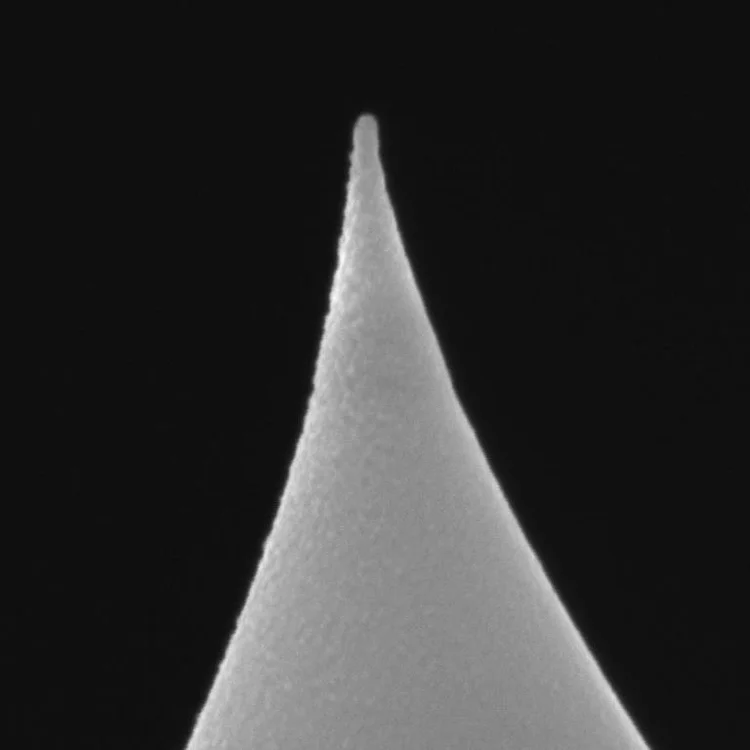
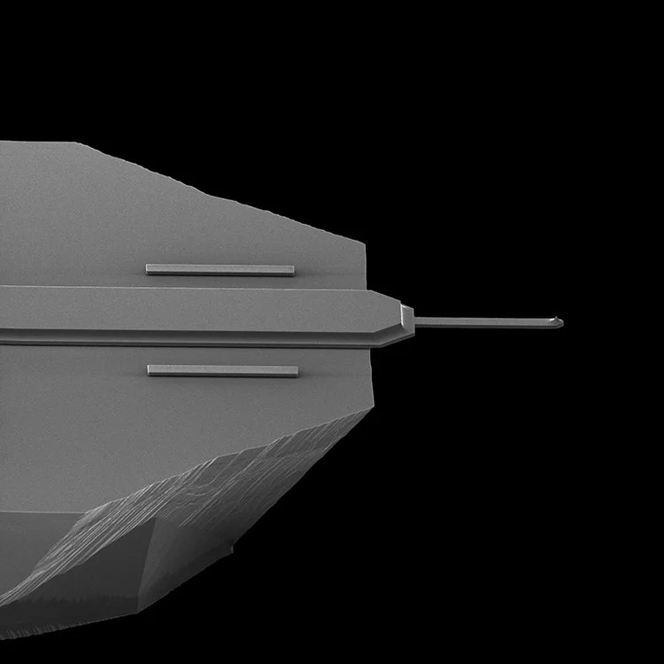
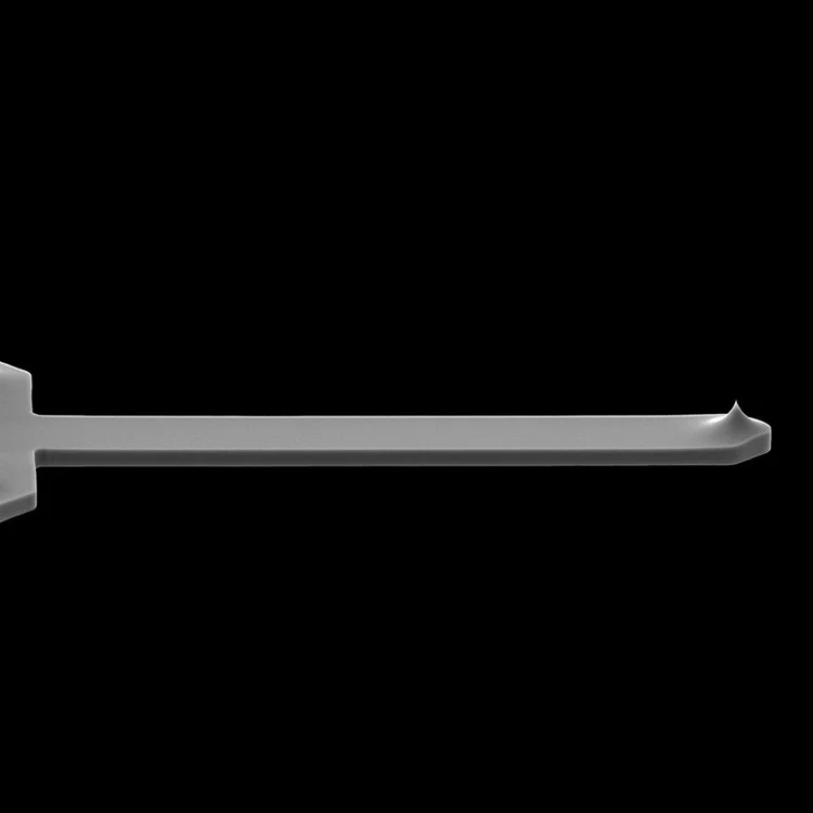
The SPARK 150 Pt is engineered to establish a highly stable electrical contact without damaging soft surfaces. Every tip is verified with SEM images for guaranteed structural integrity.
| Cantilever Specifications | |
|---|---|
| Material & Doping | silicon n‑type antimony doped, resistivity 0.015–0.025 Ω·cm |
| Cantilever Shape | spark 150 pt rectangular cantilever 225 µm |
| Spring Constant | conductive afm spring constant 18 n/m (Range: 5 - 25 N/m) |
| Resonant Frequency | afm resonant frequency 150 khz (Range: 120 - 170 kHz) |
| Length | afm cantilever length 225 µm (Range: 223 - 227 µm) |
| Width | 30 µm (Range: 28 - 32 µm) |
| Thickness | 5.5 µm (Range: 5.0 - 6.0 µm) |
| Reflective Backside Coating | platinum reflective 40 nm Pt + 5 nm Ti backside |
| Tip Specifications (Conductive) | |
| Tip Shape | afm conical tip cone angle 25° (Range: 15° - 40°) |
| Frontside Tip Coating | platinum coating 40 nm Pt + 5 nm Ti frontside/tip |
| Tip Radius | Nominal 18 nm (Guaranteed spark 150 pt tip radius <30 nm) |
| Tip Height | spark 150 pt tip height 12 µm (Range: 10 - 13 µm) |
| Tip Setback | spark 150 pt setback 7.5 µm (Range: 6.5 - 8.5 µm) |
| Packaging & Quality Assurance | |
| Quantity | conductive afm pack 10 sem imaged |
| Quality Control | individual sem images conductive tips provided for every probe |
Key Applications: Electrical Characterization on Soft Samples
-
Kelvin Probe Force Microscopy (SKPM) The dual Pt coating ensures a highly stable work function. This makes it the premier kelvin probe polymers pt coated tool for skpm tapping conductive polymers and delicate films.
-
Conductive AFM (c-AFM) & PtIR Highly effective for localized current mapping on soft matter. Operates beautifully as a c‑afm ac mode soft air instrument and a ptir afm soft thin films probe.
-
Polymers & Biomolecules With a flexible 18 N/m cantilever, it is ideal for conductive afm polymers electrical analysis, enabling precise electrical mapping biomolecules without physically damaging the delicate samples.
Frequently Asked Questions: Conductive AFM Probes
The SPARK 150 Pt is a specialized conductive afm probe softer samples model. It is expressly designed for electrical characterization in AC modes (non-contact/tapping) on delicate materials, excelling in SKPM, c-AFM, and PtIR mapping without damaging soft substrates.
This platinum coated afm probe features a robust 40 nm Pt + 5 nm Ti coating on both the frontside tip and the backside. This ti pt afm conductive cantilever design guarantees an uninterrupted electrical pathway and supreme laser reflectivity.
It operates with a lower spark 150 pt 18 n/m spring constant and a spark 150 pt 150 khz resonant frequency. These specific mechanics make it the perfect c‑afm probe low force instrument for conductive tapping afm soft materials.
Even with the dense metallic layers required for conductivity, the spark 150 pt conical tip radius is exceptionally fine at a nominal 18 nm, guaranteeing a tip radius <30 nm for precise nanoscale electrical mapping.
Yes, to ensure the highest standard of quality control, every spark 150 pt conductive afm probes pack 10 includes spark 150 pt sem images each tip, guaranteeing a reliable, low dud rate experience.
To buy spark 150 pt afm probes, submit a quote request via our contact form. We will quickly provide the exact nunano spark 150 pt price in India, including bulk spark 150 pt afm tips costs.