Written by GBS Technical Team — Scientific Instrument Specialists Since 2021 · Last updated: May 2026
What Is EDS — And What Does It Actually Measure?
Every element in the periodic table emits X-rays at specific, characteristic energies when its atoms are excited by a high-energy electron beam. This is the physical principle behind EDS. When the SEM’s electron beam hits the sample, it ejects inner-shell electrons from atoms in the material. As outer-shell electrons fall in to fill the vacancy, they release the energy difference as an X-ray — at an energy that is unique to that element.
The EDS detector sits close to the sample inside the SEM chamber and counts these X-rays, sorting them by energy. The result is a spectrum: a graph where each peak corresponds to an element. The energy position of the peak identifies the element; the peak height (intensity) reflects its relative concentration. Oxford Instruments and Bruker software then applies corrections to convert raw intensities into accurate elemental concentrations in weight percent (wt%) and atomic percent (at%).
In plain terms: SEM shows you what a material looks like at the nanoscale. EDS tells you what it is made of. Together they answer most materials characterisation questions in a single instrument session.
EDS spectrum from SEM elemental analysis — each peak corresponds to a specific element. Peak energy position identifies the element; peak intensity quantifies its concentration. This type of spectrum is generated using the Oxford AZtec or Bruker ESPRIT software integrated with the Module Sci PV-100 SEM from GBS.
How EDS Works — The 4-Step Process
01
Electron Beam Excitation
The SEM’s focused electron beam strikes the sample surface. High-energy electrons in the beam knock inner-shell electrons out of atoms in the material, creating unstable “excited” atoms.
02
Characteristic X-Ray Emission
An outer-shell electron falls into the inner-shell vacancy, releasing the energy difference as an X-ray photon. The X-ray energy is characteristic — unique to the specific element and the specific shell transition.
03
X-Ray Detection
The EDS detector (silicon drift detector, or SDD) measures the energy of each incoming X-ray. Thousands of X-rays are counted per second, building up the energy spectrum. Oxford XMax and Bruker XFlash detectors both use SDD technology.
04
Spectrum Analysis & Quantification
Software (Oxford AZtec or Bruker ESPRIT) identifies elemental peaks from the spectrum, deconvolutes overlapping peaks, and applies ZAF correction to convert intensities into accurate weight percent concentrations.
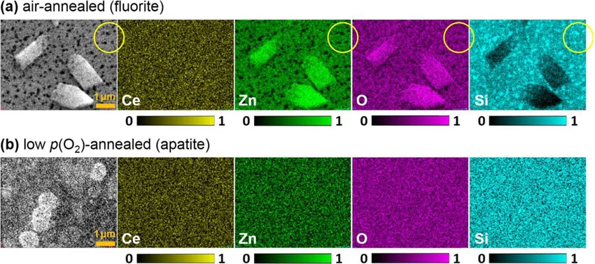
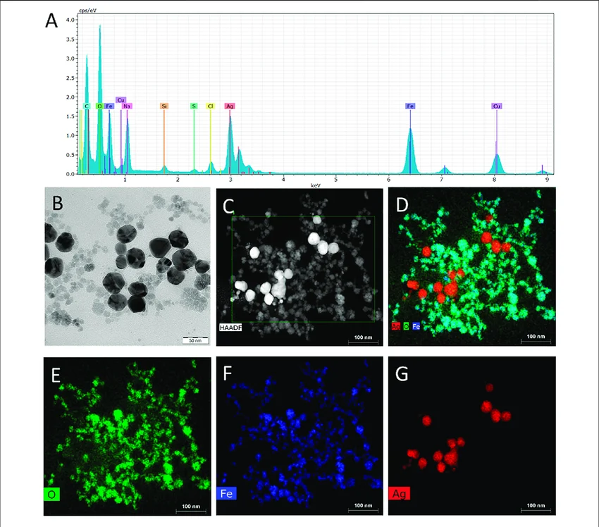
EDS elemental maps showing the distribution of Ce (cerium), Zn (zinc), O (oxygen), and Si (silicon) across the sample area. Each colour corresponds to one element — red regions are cerium-rich, green regions are zinc-rich. This simultaneous multi-element mapping is possible with Oxford AZtec and Bruker ESPRIT software integrated with the Module Sci PV-100.
4 EDS Analysis Modes — What You Can Do
01
Point Analysis
Place the electron beam at a single user-selected spot on the sample. EDS collects X-rays from that location and produces a full elemental spectrum with quantification. Identifies what a specific feature, inclusion, or particle is made of in under 60 seconds.
Best for: Inclusion identification, phase confirmation, contamination spot analysis, foreign particle investigation
02
Elemental Mapping
The electron beam scans across the entire image area, collecting X-rays at every pixel. Each element is displayed as a colour-coded map showing its spatial distribution across the sample. Up to 10+ elements can be mapped simultaneously.
Best for: Phase distribution in alloys, segregation at grain boundaries, coating layer identification, composite filler distribution
03
Line Scan
EDS data is collected along a user-defined straight line across the sample. The result is a concentration profile — a graph showing how each element’s concentration changes across an interface, layer boundary, or gradient zone.
Best for: Coating-substrate interface, diffusion profiles, multilayer film analysis, weld heat-affected zone composition
04
Quantitative Area Analysis
EDS data from a defined area is integrated to produce a bulk elemental composition — weight percent and atomic percent for each element present. ZAF correction is applied for accuracy. Results are table-format and can be exported for reports and publications.
Best for: Alloy composition verification, bulk phase quantification, regulatory submissions, comparative batch analysis
Oxford Instruments vs Bruker — Which EDS for Your PV-100?
The Module Sci PV-100 SEM from GBS is compatible with EDS detectors from both Oxford Instruments and Bruker — the two leading EDS manufacturers globally. Both produce silicon drift detectors (SDD) that deliver excellent energy resolution and fast acquisition. Here is a detailed comparison to help you choose.
Oxford Instruments
AZtec EDS System · XMax Detector
- Market-leading AZtec software — most feature-rich EDS platform
- Automated phase mapping (AutoPhaseMap) — identifies distinct phases
- TruMap — background-subtracted elemental maps for cleaner results
- Particle analysis — automated feature detection and classification
- Large active area detector options for fast map acquisition
- Widely used in Indian research institutions — familiar software
- Full compatibility confirmed with Module Sci PV-100
Best for: Complex multi-phase analysis, automated particle analysis, research publication work requiring advanced software features
Bruker
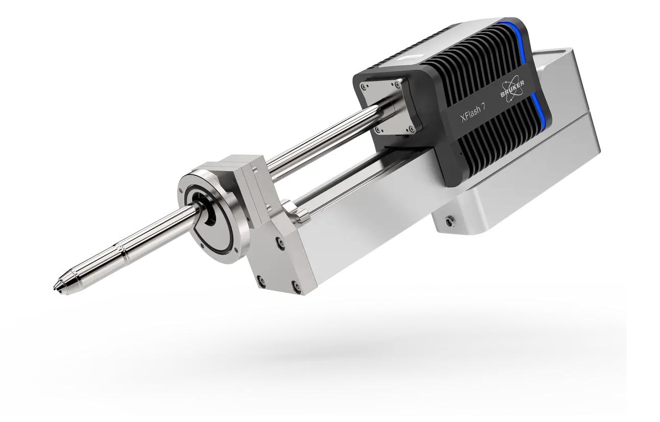
Quantax EDS · XFlash 7 Detector
- XFlash 7 — highest energy resolution SDD available (< 121 eV FWHM at Mn Kα)
- Fast acquisition — excellent count rates for rapid mapping
- ESPRIT software — clean, intuitive interface for industrial users
- Excellent light element detection (C, N, O, F at low concentrations)
- Quantax Phase Analysis — automated phase segmentation
- Strong in industrial QC environments — fast, reliable, robust
- Full compatibility confirmed with Module Sci PV-100
Best for: Industrial QC requiring fast throughput, light element analysis, carbon/nitrogen/oxygen detection in materials, labs prioritising acquisition speed
GBS recommendation: For most Indian research labs (universities, IITs, IISc), Oxford AZtec is the preferred choice due to its advanced phase mapping and particle analysis features that directly support publication-quality analysis. For industrial QC labs (automotive, energy, semiconductor) where speed and throughput matter more than advanced software features, Bruker XFlash is an excellent choice. Contact GBS to discuss which system best fits your specific application before ordering.
ZAF Correction — Why Raw EDS Intensities Are Not Concentrations
Raw EDS X-ray intensities cannot be directly converted to elemental concentrations. Three physical effects distort the relationship between X-ray count and actual elemental concentration. ZAF correction accounts for all three, and is applied automatically by both Oxford AZtec and Bruker ESPRIT software.
Z
Atomic Number Correction
Heavier elements (higher Z) absorb the incident electron beam more strongly, generating fewer X-rays per unit mass. Z correction accounts for this stopping power difference between elements in the sample.
A
Absorption Correction
X-rays generated deep in the sample must travel through the material to reach the detector — and are partially absorbed on the way. A correction accounts for X-ray absorption, which is especially significant for light element analysis.
F
Fluorescence Correction
X-rays from one element can excite secondary X-ray emission from another element in the sample (fluorescence). F correction removes this artifact, which is most significant when high-energy emitters are adjacent to lower-energy emitters in the same sample.
The Single Most Important EDS Rule — Carbon Not Gold
This rule prevents the most common and most damaging EDS mistake made in Indian labs every week. Understanding it takes 60 seconds; not knowing it can ruin an entire analysis session.
⚠️ Gold Sputter Coating
Only for SEM imaging — never for EDS
- ✓ Excellent for SE imaging — high secondary electron yield, sharp images
- ✓ Non-conductive samples: polymers, ceramics, biological
- ✗ Introduces Au Mα peak at ~2.1 keV — overlaps with S Kα and Mo Lα
- ✗ Introduces Au Lα peak at ~9.7 keV — overlaps with Zn Kβ
- ✗ Cannot detect sulfur, molybdenum reliably in gold-coated samples
- ✗ EDS quantification results will be wrong — gold appears as false element
VS
✅ Carbon Sputter Coating
Required whenever EDS analysis is needed
- ✓ Carbon Kα peak at 0.277 keV — does not interfere with any element above boron
- ✓ All elements of interest are detectable without interference
- ✓ EDS quantification results are accurate
- ✓ Slightly lower image contrast than gold — acceptable for most applications
- ✓ GBS supplies Quorum carbon coaters alongside the PV-100
- ✗ Slightly lower secondary electron yield than gold — marginally lower image contrast
Remember: If someone in your lab coats a sample with gold and then tries to run EDS — the gold peaks will appear in the spectrum, sulfur and molybdenum will be undetectable, and all quantification results will be wrong. The sample must be cleaned and re-coated with carbon. This wastes hours and damages samples. Always check coating type before loading for EDS.
SEM-EDS Applications Across Indian Industries
| Sector | SEM-EDS Application | What EDS Adds vs SEM Alone | Indian Users |
|---|
| Materials Science |
Alloy composition, phase mapping, inclusion analysis |
Identifies what each phase is — SEM shows where, EDS shows what |
IISc, IIT Bombay, JNCASR |
| Failure Analysis |
Corrosive species at fracture sites, contamination ID |
Elemental identity of corrosion deposits, foreign inclusions, fracture trigger particles |
GE Vernova, Hyundai Mobis |
| Pharmaceutical QC |
Foreign particle elemental ID, coating composition |
Confirms whether contamination is organic (C, N, O) or inorganic (metals, silica) |
Himalaya, Aurigene, Syngene |
| Semiconductor |
Wafer contamination, bonding interface, solder composition |
Identifies contamination elements; maps intermetallic compound formation |
Semiconductor fabs, OSAT facilities |
| Geology & Mineralogy |
Mineral identification, ore grade assessment |
EDS identifies mineral phases by elemental composition — replaces XRD for single-grain analysis |
CSIR-NGRI, mining research |
| Ceramics & Glass |
Phase mapping, grain boundary chemistry, sintering analysis |
Maps element segregation at grain boundaries — explains mechanical and electrical properties |
Advanced ceramics R&D labs |
| Automotive |
Coating composition, plating thickness, weld verification |
Confirms coating alloy composition; identifies unexpected elements causing corrosion |
Hyundai Mobis, Tata, Mahindra supply chain |
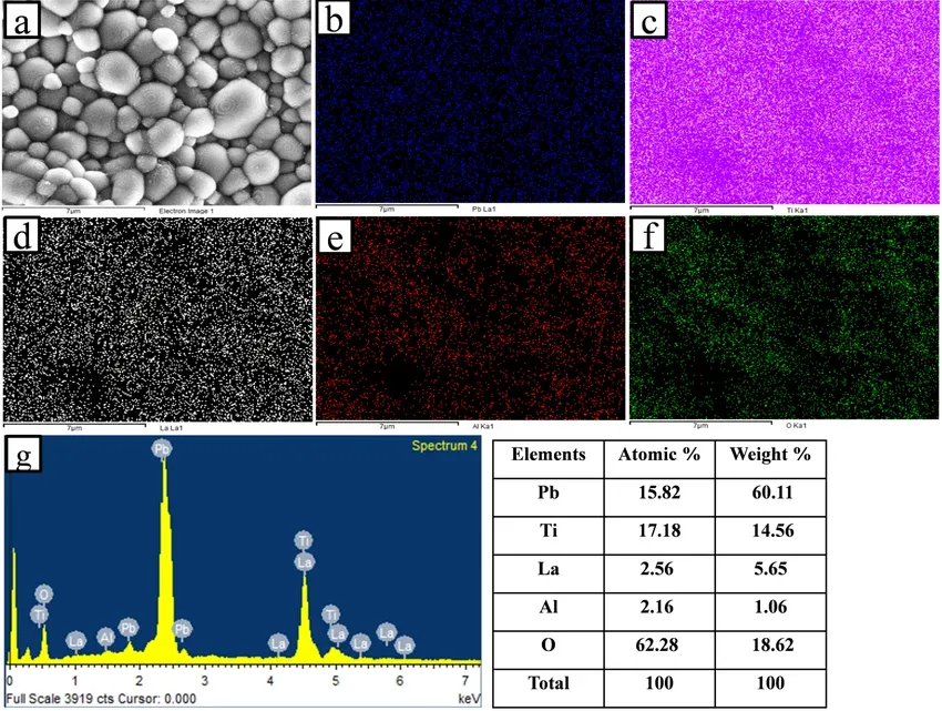
SEM-EDS elemental map of perovskite ceramic (Pb, La, Ti, Al, O) — phase distribution mapped simultaneously across the sample area
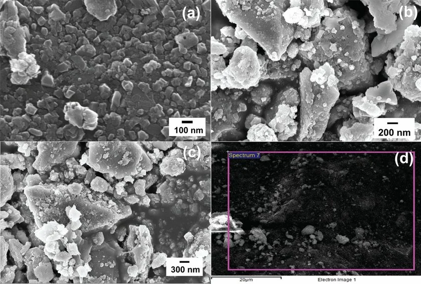
SEM + EDAX analysis of steel slag — surface morphology (a, b, c) and elemental spectrum (d) confirm slag composition
How GBS Supplies SEM + EDS Together in India
GBS supplies the Module Sci PV-100 SEM and EDS detector as an integrated system — not two separate purchases from different suppliers. This matters for three reasons:
✅ Pre-verified compatibility
GBS tests the PV-100 + EDS combination before delivery. Interface connections, software integration, and detector geometry are verified against the specific PV-100 unit — eliminating the compatibility uncertainty that arises when customers source SEM and EDS from different vendors.
✅ Single installation visit
The GBS engineer installs both the PV-100 SEM and the EDS detector in the same visit — calibrating the full system, running standard reference spectra to verify EDS performance, and training operators on both the SEM imaging and EDS analysis workflows in one session.
✅ Single AMC covers both instruments
The GBS Annual Maintenance Contract covers the PV-100 SEM and EDS detector together. Annual PM visits include detector performance checks, EDS calibration on reference standards, and software updates for both AZtec/ESPRIT and Module Sci control software — one visit, one report, one contract.
GBS locations for SEM + EDS service: Bengaluru (HQ) · Noida · Kanpur. Service engineers based in all three cities. Contact
service@globalbiosciencesolution.com for AMC pricing for a PV-100 + EDS system.
Frequently Asked Questions
What is EDS in SEM and what does it measure?
EDS (Energy Dispersive Spectroscopy) identifies which chemical elements are present in a sample by detecting characteristic X-rays emitted when the SEM electron beam strikes the material. Each element emits X-rays at specific, unique energies — the EDS detector measures these and produces a spectrum where each peak identifies one element. Software then quantifies concentrations in weight percent. EDS detects elements from beryllium (Z=4) to uranium (Z=92). The Module Sci PV-100 SEM from GBS supports EDS detectors from Oxford Instruments and Bruker.
What is the difference between Oxford Instruments and Bruker EDS detectors?
Both are excellent and fully compatible with the PV-100. Oxford Instruments AZtec is the market leader with the most advanced software — AutoPhaseMap, TruMap, and automated particle analysis make it the preferred choice for research and complex multi-phase work. Bruker XFlash 7 offers the highest energy resolution (<121 eV FWHM) and fastest count rates — ideal for industrial QC labs and light element detection (C, N, O, F). Contact GBS to discuss which suits your specific applications before ordering.
Why do I need carbon coating for EDS and not gold?
Gold must never be used for EDS samples. Gold produces strong X-ray peaks at ~2.1 keV (overlaps with sulfur Kα) and ~9.7 keV (overlaps with zinc Kβ) — making sulfur, molybdenum, and other elements undetectable. All quantification results are corrupted by the gold signal. Carbon coating (5–8 nm) produces only a very weak 0.277 keV peak that does not interfere with any element above boron. GBS supplies Quorum carbon sputter coaters alongside the PV-100 — both from the same supplier.
Can the Module Sci PV-100 do EDS elemental mapping?
Yes. With an Oxford or Bruker EDS detector integrated, the Module Sci PV-100 performs: point analysis (elemental composition at a spot), area elemental mapping (colour-coded element distribution), line scans (concentration profile across an interface), and full quantification with ZAF correction. GBS supplies and installs the complete PV-100 + EDS system from Bengaluru with a single installation visit and AMC.
What are the main applications of SEM-EDS in India?
Key SEM-EDS applications in India: materials science (alloy composition, phase mapping, inclusion ID), failure analysis (corrosion species, contamination ID), pharma QC (foreign particle elemental analysis, coating composition), semiconductor inspection (wafer contamination, bonding interfaces), geology (mineral identification), ceramics (grain boundary chemistry), and automotive QC (coating composition, weld verification). GBS supplies PV-100 + EDS to IISc, IIT Bombay, GE Vernova, Hyundai Mobis, and pharma customers.
What elements can SEM-EDS detect?
EDS detects elements from beryllium (Be, Z=4) to uranium (U, Z=92). In practice, elements lighter than carbon are difficult to detect reliably due to low X-ray energy absorption. Minimum detectable concentration: typically 0.1–0.5 weight percent for major elements under standard conditions — suitable for major and minor element analysis. Trace elements below 0.1 wt% require WDS (Wavelength Dispersive Spectroscopy) on an electron probe microanalyser — a more specialised instrument.
How much does a SEM with EDS cost in India?
The Module Sci PV-100 base SEM is ₹60 lakh. EDS detector integration (Oxford or Bruker) adds to the system price — contact GBS at +91 97436 20456 or sales@globalbiosciencesolution.com for current PV-100 + EDS bundle pricing. The complete system remains significantly more cost-effective than full-size SEM+EDS setups (₹1.5 crore to ₹3 crore+).
What is ZAF correction in EDS quantification?
ZAF correction converts raw EDS X-ray intensities into accurate elemental concentrations. Z corrects for atomic number effects (heavier atoms absorb more electrons). A corrects for X-ray absorption within the sample before reaching the detector. F corrects for fluorescence — secondary X-rays from one element exciting another. Without ZAF correction, raw intensities are not accurate concentrations. Both Oxford AZtec and Bruker ESPRIT software apply ZAF correction automatically. Results are reported as weight percent (wt%) and atomic percent (at%).
References & External Sources
Get the Module Sci PV-100 with EDS in India
GBS supplies the complete PV-100 + EDS system from Bengaluru — Oxford Instruments or Bruker, installed and calibrated together, single AMC. Contact us for bundle pricing.