Written by GBS Technical Team — Scientific Instrument Specialists Since 2021 · Last updated: April 2026
Why SEM Is Central to Materials Science Research in India
Materials science is fundamentally a visual discipline. The properties of a material — its strength, conductivity, corrosion resistance, optical behaviour — are determined by its microstructure: the arrangement of grains, phases, interfaces, defects, and inclusions at the micron and nanometre scale. SEM makes this microstructure visible.
India’s materials science research community has grown rapidly over the past decade. IISc Bangalore and the IITs are publishing world-class research on nanomaterials, energy materials, and advanced composites. At the same time, Indian industry — automotive, energy, semiconductor, aerospace — is building in-house materials testing capability rather than outsourcing to external labs at ₹5,000–10,000 per SEM run. The tabletop SEM revolution has made this accessible: for ₹60 lakh, any research lab or industrial QC facility can own a system with 300,000x magnification and EDS capability that was previously only available to well-funded central facilities.
The tabletop SEM advantage for Indian materials labs: A full-size SEM costs ₹80 lakh–₹2 crore, requires a dedicated 15–25 sqm room, and needs a specialist operator. The Module Sci PV-100 costs ₹60 lakh, sits on a lab bench (0.5 sqm), and can be operated by any trained researcher. For 90% of materials science applications — nanoparticle imaging, fracture analysis, coating inspection, ceramic microstructure — the tabletop system is fully sufficient.
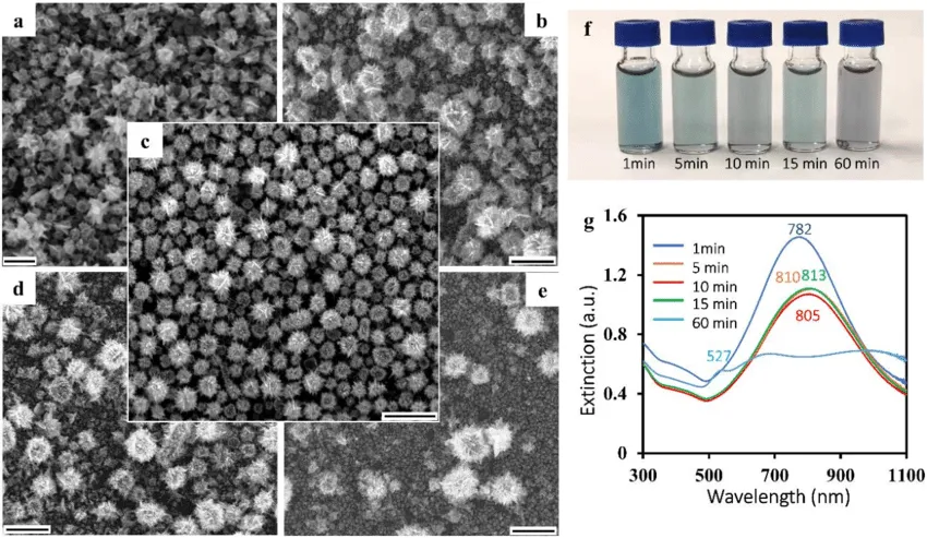
SEM images of Au-Ag alloy nanoparticles (a–e) showing particle morphology, size distribution, and agglomeration state. This type of high-resolution nanoparticle characterisation is performed using the Module Sci PV-100 tabletop SEM, supplied by GBS India.
6 Core Materials Science Applications for SEM in India
🔬
Nanoparticle Imaging
Metal, Oxide, Semiconductor & Polymer Nanoparticles
SEM is one of the primary techniques for nanoparticle characterisation — providing direct morphological evidence of particle shape, size distribution, surface texture, and agglomeration state that light scattering techniques cannot resolve.
- Gold, silver, platinum nanoparticles — morphology and size distribution
- Iron oxide (Fe₃O₄) nanoparticles for biomedical applications
- Semiconductor quantum dots (ZnO, TiO₂, CdS)
- Agglomeration vs individual particle differentiation
- Nanoparticle synthesis quality control — confirm target morphology
- EDS for composition verification alongside morphology
🏛️ IISc · IIT Bombay · JNCASR Nanotechnology Research
🔩
Metal Fracture Analysis
Failure Analysis · Fracture Mechanics · Weld Inspection
Fracture surface morphology reveals the mechanism of failure — ductile vs brittle fracture, fatigue crack initiation sites, stress corrosion cracking, and weld defects. SEM provides the high-resolution fractographic evidence required for failure investigation reports.
- Ductile fracture — dimple morphology and void coalescence
- Brittle fracture — cleavage facets and transgranular vs intergranular mode
- Fatigue striations — crack propagation rate estimation
- Weld quality — porosity, incomplete fusion, HAZ microstructure
- Corrosion morphology — pitting, stress corrosion, galvanic attack
- EDS for identifying corrosive species at failure sites
🏭 GE Vernova · Hyundai Mobis · Industrial Failure Analysis
🧱
Ceramic Microstructure
Grain Structure · Phase Distribution · Sintering Quality
Ceramic performance is controlled by grain size, grain boundary chemistry, phase distribution, and porosity — all of which are directly characterised by SEM. The EDS elemental mapping capability is particularly valuable for multi-phase ceramics and functional ceramic materials.
- Grain size measurement and distribution in sintered ceramics
- Intergranular vs transgranular fracture mode identification
- Phase mapping of multi-component ceramics (EDS required)
- Porosity assessment — open vs closed pore structure
- Piezoelectric ceramics (PZT, BaTiO₃) — domain structure
- Sintering quality verification — neck formation between grains
🏛️ IISc Materials Engineering · Advanced Ceramics Research
🧩
Composite Characterisation
Fibre-Matrix Interface · Delamination · Void Analysis
The mechanical performance of composite materials depends critically on the quality of the fibre-matrix interface, fibre distribution, and void content. SEM cross-section imaging provides direct visual evidence of these parameters — essential for both research and industrial quality assurance.
- Carbon fibre / glass fibre — matrix adhesion and interfacial bonding
- Fibre pull-out vs matrix cracking failure mode identification
- Void content and distribution in cured composites
- Delamination initiation and crack path in layered composites
- Nanocomposite filler dispersion (clay, graphene, CNT) in polymer matrix
- EDS mapping for filler distribution and interfacial chemistry
🔬 Polymer Composites · Aerospace Materials · Automotive
🎨
Coating Analysis
Thickness · Adhesion · Porosity · Defect Detection
Coating performance in corrosion protection, thermal barrier, and optical applications depends on thickness uniformity, porosity, and adhesion. SEM cross-sections and surface imaging provide quantitative coating characterisation that profilometry and optical methods cannot match.
- Thermal spray coating — lamellar structure and porosity
- PVD/CVD thin film thickness measurement from cross-section
- Electroplating uniformity — thickness variation and pinhole detection
- Anti-corrosion coating adhesion and delamination inspection
- Optical coating defects — pinholes, nodules, cracks
- EDS for coating composition and interface diffusion measurement
🏭 Surface Engineering · Protective Coatings · Thin Films
💻
Semiconductor & Electronics Inspection
Surface Defects · Via Fill · Bonding Interfaces
India’s growing semiconductor and electronics manufacturing sector requires in-house materials inspection capability. SEM provides nanoscale surface and cross-section inspection for semiconductor wafers, PCB structures, and bonding interfaces — applications set to grow rapidly with India’s PLI-driven fab expansion.
- Wafer surface defect inspection — particles, scratches, hillocks
- Via fill quality in PCB and semiconductor interconnects
- Wire bonding interface — intermetallic compound formation
- Solder joint quality — void content, intermetallic thickness
- MEMS device characterisation — structural features at micron scale
- EDS for contamination identification on wafer surfaces
🇮🇳 India Semiconductor PLI · Electronics Manufacturing
EDS Elemental Mapping — The Power of SEM + Chemistry
SEM imaging tells you what a material looks like at the nanoscale. EDS tells you what it is made of. Together, they provide the complete picture that materials scientists and failure analysts need.
EDS · Oxford Instruments · Bruker · Compatible with PV-100
SEM-EDS Elemental Mapping for Materials
The Module Sci PV-100 SEM from GBS is fully compatible with EDS detectors from Oxford Instruments and Bruker — enabling elemental composition analysis alongside surface imaging without changing instruments.
- Point analysis — elemental composition at a specific location
- Area mapping — colour-coded element distribution across the entire image
- Line scan — elemental concentration profile across an interface
- Quantification — weight% and atomic% with ZAF correction
- Phase identification — map phases by their elemental signature
- Inclusion and contamination identification in metals and ceramics
- Diffusion profile measurement across bonding interfaces
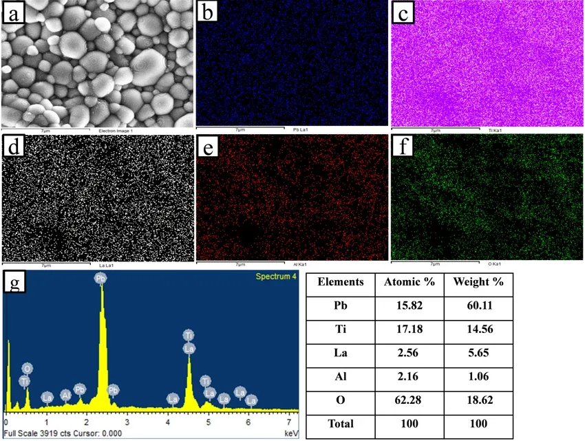
SEM-EDS elemental map of perovskite ceramic showing Pb, La, Ti, Al distribution
Gold vs carbon coating for EDS: If you need EDS elemental analysis alongside SEM imaging, always use
carbon sputter coating — not gold. Gold introduces strong Au X-ray peaks (~2.1 keV and ~9.7 keV) that overlap with and mask other elements of interest. Carbon coating is transparent to EDS and will not affect your elemental spectrum. GBS supplies
Quorum sputter coaters alongside the PV-100.
SEM Analysis of Industrial Materials — Steel Example
The following SEM and EDAX analysis of steel slag demonstrates the type of multi-modal surface morphology and elemental characterisation that the Module Sci PV-100 enables for industrial and research samples.
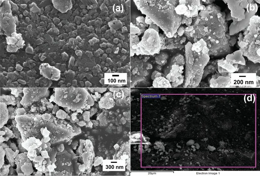
SEM analysis of steel slag: panels (a), (b), (c) — surface morphology at increasing magnification; panel (d) — EDAX elemental spectrum confirming slag composition. This type of analysis is performed using the Module Sci PV-100 + EDS setup from GBS.
This multi-panel SEM+EDAX analysis of steel slag is representative of the analytical workflow used at Indian industrial facilities. Panel (d) shows the EDAX spectrum — the characteristic X-ray peaks identify each element present, while the intensity quantifies their relative concentration. GE Vernova and Hyundai Mobis use GBS-supplied instruments for exactly this type of in-house materials characterisation.
Indian Institutions & Industries Using GBS SEM for Materials Science
IISc Bangalore
Premier Research Institution
India’s top-ranked research university with world-class departments in materials engineering, solid state and structural chemistry, and nanoscience. Uses GBS-supplied instruments for advanced materials characterisation across multiple departments.
- Nanomaterials synthesis characterisation
- Ceramic and metal microstructure research
- Thin film and coating analysis
SEMEDSBengaluru
IIT Bombay
IIT — Materials & Chemical Engineering
Leading IIT with strong materials science and chemical engineering research groups. Uses GBS instruments for nanomaterials, energy materials, and composites research — supporting publications in Nature Materials, ACS Nano, and Advanced Materials.
- Energy material microstructure (batteries, solar cells)
- Nanoparticle synthesis and characterisation
- Composite materials failure analysis
SEMNanoparticlesMumbai
GE Vernova India
Energy Equipment Manufacturer
Global energy technology company with significant India manufacturing and R&D operations. Uses GBS-supplied SEM for in-house materials testing of turbine components, insulator materials, and energy equipment — reducing dependence on external testing labs.
- Turbine component surface inspection
- Insulator material failure analysis
- Metal alloy microstructure verification
SEM + EDSFailure AnalysisIndustrial
Hyundai Mobis India
Automotive Components Manufacturer
Leading automotive parts manufacturer with India production facilities. Uses GBS-supplied instruments for materials testing of automotive components — metal surface inspection, coating quality analysis, and failure analysis of returned parts.
- Automotive component fracture surface analysis
- Protective coating quality inspection
- Metal surface defect characterisation
SEMCoatingsAutomotive QC
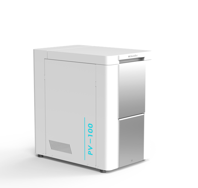
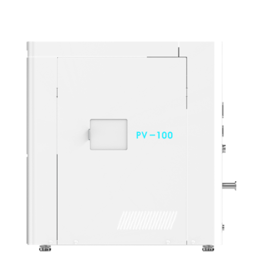
Module Sci PV-100 Series — Table-Top W-SEM · ₹60 lakh · Supplied by GBS India
PV-100 imaging results — 304 steel 2,000x · AlN whiskers 5,000x · paper 10,000x · powder 2,000x
Module Sci PV-100 — Specifications for Materials Science
The following specifications are directly relevant to materials science applications. For the complete technical specification including all parameters, see the PV-100 full specifications page.
| Parameter | PV-100 Specification | Materials Science Relevance |
|---|
| Magnification range |
20x to 300,000x |
Covers low-mag grain overview (200x) through nanoparticle imaging (100,000x+) |
| Imaging modes |
Secondary Electron (SE) + Backscattered Electron (BSE) |
SE for topography; BSE for phase/composition contrast in multi-phase materials |
| Stage type |
Motorised 5-axis (X, Y, Z, Rotation, Tilt) |
Tilt stage enables cross-section imaging and 3D perspective of fracture surfaces |
| Sample exchange |
Sub-60 seconds |
High-throughput materials studies — multiple samples per session without long waits |
| EDS compatibility |
Oxford Instruments + Bruker |
Full elemental mapping, quantification, and phase analysis alongside SEM imaging |
| Sample preparation required |
Conductive: none. Non-conductive: gold or carbon sputter coat. |
Most metals and semiconductors: load directly. Ceramics, polymers, composites: coat first. |
| Footprint |
Tabletop (standard bench) |
Fits in existing lab space — no dedicated SEM room needed |
| Price (India) |
₹60 lakh |
Most cost-effective 300,000x + EDS-compatible SEM available in India with local service |
Frequently Asked Questions
How is SEM used in materials science research in India?
SEM is used for six core applications in Indian materials science: nanoparticle imaging (morphology, size, agglomeration), metal fracture analysis (fracture mode, fatigue striations, grain boundaries), composite characterisation (fibre-matrix interface, void content), coating analysis (thickness, porosity, adhesion), ceramic microstructure (grain size, phase distribution, sintering quality), and semiconductor inspection (surface defects, via fill, bonding interfaces). IISc Bangalore, IIT Bombay, GE Vernova, and Hyundai Mobis use GBS-supplied SEM for these applications.
What is EDS and how does it complement SEM in materials science?
EDS (Energy Dispersive Spectroscopy) identifies the chemical elements in a sample by detecting characteristic X-rays when the electron beam hits the material. SEM shows what the surface looks like; EDS shows what it is made of. In materials science, EDS enables elemental composition maps (colour-coded element distribution), point analysis of specific phases, line scans across interfaces, and elemental quantification. The Module Sci PV-100 from GBS is compatible with Oxford Instruments and Bruker EDS detectors.
What is the best SEM for materials science research in India?
For most Indian university and industrial materials science labs, the Module Sci PV-100 tabletop SEM from GBS is the recommended choice. At ₹60 lakh, it offers 300,000x magnification, motorised 5-axis stage, sub-60-second sample exchange, and full EDS compatibility — sufficient for all standard materials characterisation. It sits on a lab bench with no dedicated room required. IISc Bangalore, IIT Bombay, NCBS, and JNCASR use GBS-supplied instruments.
Can SEM image nanoparticles?
Yes. SEM is one of the primary techniques for nanoparticle characterisation. The PV-100 images nanoparticles at up to 300,000x, resolving individual particle morphology, size distribution, surface texture, and agglomeration. Metallic nanoparticles (gold, silver, platinum) require no coating. Non-conductive nanoparticles (silica, ceramic, polymer) require a thin carbon or gold sputter coat. EDS confirms nanoparticle composition and detects impurities simultaneously. See the Quorum sputter coaters available from GBS.
Does SEM need sample preparation for metals and alloys?
Conductive samples — most metals, alloys, and semiconductors — require no coating and can be loaded directly into the PV-100. Non-conductive materials (ceramics, polymers, composites) require gold coating (imaging only) or carbon coating (if EDS is needed). For EDS on any sample, always use carbon coating — gold introduces Au peaks that interfere with the elemental spectrum. GBS supplies Quorum Technologies sputter coaters alongside the PV-100.
What is the price of a tabletop SEM for materials science in India?
The Module Sci PV-100 is priced at ₹60 lakh. Full-size SEM systems (Hitachi, JEOL, Thermo Fisher) cost ₹80 lakh to ₹2 crore+ and require dedicated rooms. For the vast majority of materials science applications, the PV-100 provides equivalent imaging capability at significantly lower cost. Contact GBS at +91 97436 20456 or sales@globalbiosciencesolution.com for current pricing.
Which Indian institutions use SEM for materials science research?
Leading Indian institutions using GBS-supplied SEM for materials science include IISc Bangalore (materials engineering, nanoscience), IIT Bombay (materials and chemical engineering), NCBS, JNCASR (advanced materials), IIT Madras, and HASETRI. Industrial users include GE Vernova (energy equipment materials testing) and Hyundai Mobis (automotive component failure analysis). GBS is headquartered in Bengaluru with branches in Noida and Kanpur — enabling India-wide service coverage.
What is the difference between SE and BSE imaging in materials science?
Secondary Electron (SE) imaging gives topographical contrast — surface morphology, texture, fracture features. Best for: fracture analysis, nanoparticle shape, coating surface. Backscattered Electron (BSE) imaging gives compositional (Z) contrast — heavier elements appear brighter. Best for: phase mapping in multi-phase alloys, inclusion detection, grain boundary contrast. The Module Sci PV-100 supports both SE and BSE imaging modes.
References & External Sources
Get a Quote for the Module Sci PV-100 SEM
GBS supplies the PV-100 tabletop SEM across India with EDS options, same-day installation, and annual service plans. Trusted by IISc, IIT Bombay, GE Vernova, and Hyundai Mobis.