

High-Precision EM Consumables
Category: Electron Microscopy Accessories
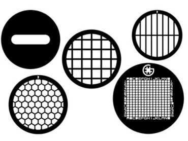
Premium TEM Grids for Transmission Electron Microscopy
Discover our extensive range of high-quality TEM grids for electron microscopy, meticulously crafted to support the most delicate nano-scale structures. Whether you require standard copper TEM grids, highly inert gold TEM grids, or specialized nickel TEM grids, our TEM specimen grids are the industry standard for stable, artifact-free imaging. We also offer specialty metals including the molybdenum tem grid and platinum tem grid for high-temperature and corrosive chemical applications.
To perfectly accommodate ultra-thin sections and nanoparticles, our laboratory TEM grids are available with superior support films. Choose from a formvar coated tem grid for robust support, a standard carbon coated tem grid, or an advanced holey carbon tem grid (and Lace carbon TEM grids) designed for cutting-edge Cryo-EM. For the absolute highest resolution, we supply the continuous carbon tem grid and ultra-thin graphene coated tem grid.
✓ 50 to 1000 Mesh Sizes ✓ Ultra-Thin Carbon ✓ Standard 3.05mm Diameter
High Purity
Metals
Metals
Formvar & Carbon
Coatings
Coatings
50 to 1000
Mesh Sizes
Mesh Sizes
Cryo-EM
Ready
Ready
Artifact-Free
Imaging
Imaging
Technical Specifications: TEM Sample Grids
Our microscopy grids for TEM are manufactured under stringent clean-room conditions to ensure absolute perfection in the mesh structure, preventing unwanted imaging artifacts.
| Grid Dimensions & Material Types | |
|---|---|
| Grid Diameter | Standard 3.05 mm (Compatible with all major TEM systems) |
| Base Metal Materials | Copper TEM grids, Gold TEM grids, Nickel TEM grids, Molybdenum tem grid, Platinum tem grid |
| Mesh Variations | Mesh TEM grids available in 50, 100, 200, 300, 400, and up to 1000 mesh. |
| Grid Styles | Square mesh, Hexagonal mesh, Parallel bar, Folding grids, Slot grids. |
| Coating & Support Films | |
| Carbon Based Films | Carbon coated TEM grids, Continuous carbon tem grid, Ultra thin carbon TEM grids |
| Polymer Based Films | Formvar coated tem grid, Formvar/Carbon stabilized. |
| Perforated / Holey Films | Holey carbon TEM grids, Lace carbon TEM grids, Quantifoil TEM grids |
| Advanced 2D Materials | Graphene coated tem grid for minimal background noise. |
Advanced Coating & Material Options
Selecting the correct grid for electron microscope is crucial based on your sample preparation protocol and the specific chemistry of your specimens.
-
Uncoated Metal Grids Standard copper TEM grids are the most widely used. However, if your sample reacts with copper or requires specific chemical treatments, we provide highly inert gold TEM grids and nickel TEM grids.
-
Carbon & Formvar Coatings For supporting ultra-thin biological sections or fragile nanomaterials, a formvar coated tem grid provides a robust plastic substrate. The addition of a carbon layer (continuous carbon tem grid) conducts heat and electrons away from the sample, stabilizing it under the electron beam.
-
Holey, Laced Carbon & Quantifoil Essential for high-contrast imaging and Cryo-EM. A holey carbon tem grid or Lace carbon TEM grids (including Quantifoil TEM grids) allows the specimen to be suspended over a hole, completely eliminating the background noise of the support film.
Research Applications
-
Biology & Life Sciences Vital TEM support grids used extensively as TEM grids for biological samples, TEM grids for virus imaging, and TEM grids for cell ultrastructure study. Our holey grids are specifically optimized as TEM grids for cryo-EM and TEM grids for protein imaging.
-
Nanotechnology The incredibly smooth surface of an ultra thin carbon TEM grid is perfect as TEM grids for nanoparticle analysis and characterizing complex TEM grids for nanomaterials.
-
Material Science & Physics Rely on our robust molybdenum tem grid and platinum tem grid options when conducting rigorous TEM grids for material science research, high-temperature treatments, or demanding TEM grids for semiconductor analysis.
Frequently Asked Questions: TEM Grids
We supply a vast array of transmission electron microscopy grids. The most common are copper TEM grids, but we also offer gold TEM grids, nickel TEM grids, as well as specialized molybdenum tem grid and platinum tem grid options for high-temperature applications.
A carbon coated tem grid is essential for stabilizing ultra-thin samples. The carbon layer dissipates heat and charge buildup under the electron beam, preventing the sample from moving or degrading during imaging.
A holey carbon tem grid (or Lace carbon TEM grids) provides a support film with microscopic holes. It is primarily used in Cryo-EM to suspend the sample in vitreous ice over the holes, avoiding the background scattering noise that a continuous film would produce.
Absolutely. For the highest resolution needs, we recommend our ultra thin carbon TEM grids or the cutting-edge graphene coated tem grid, which provides the thinnest possible support structure with near-zero background interference.
To get a detailed quotation for any of our electron microscopy grids, including bulk orders of laboratory TEM grids, please use the contact form on this page or message us directly on WhatsApp. We will provide a comprehensive price list quickly.