
Conductive AFM Probes
Category: NuNano Conductive Probes
NuNano SPARK 350 Pt Conductive AFM Probe | Electrical Characterization
The NuNano SPARK 350 Pt is a premium conductive afm probe engineered for comprehensive electrical characterization on robust samples. Acting as the conductive counterpart to the SCOUT 350, it thrives in conductive afm probe ac mode and tapping mode, delivering exceptionally low-noise electrical signals for advanced metrology.
Manufactured from silicon n type antimony doped material, this platinum coated afm probe features a dual 40 nm pt 5 nm ti coating applied to both the frontside tip and backside. Boasting a spark 350 pt 42 n/m spring constant and a sharp tip radius <30 nm, it is the ultimate skpm afm probe and c-afm probe for complex semiconductor and thin-film analysis.
✓ SEM Imaged Tips ✓ High Conductivity ✓ Pack of 10 Probes
40nm Pt + 5nm Ti
Dual Coating
Dual Coating
42 N/m
Spring Constant
Spring Constant
350 kHz
Frequency
Frequency
SEM Imaged
Tips Included
Tips Included
Tapping Mode
Conductive
Conductive
Technical Specifications: NuNano SPARK 350 Pt
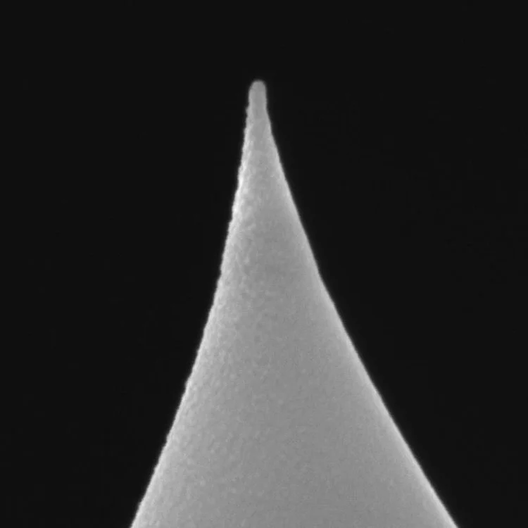
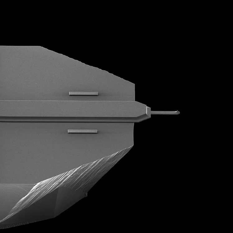
The SPARK 350 Pt is engineered to establish a highly stable electrical contact while retaining exceptional topographical resolution. Every tip is verified with SEM images for absolute precision.
| Cantilever Specifications | |
|---|---|
| Material & Doping | silicon n type antimony doped, resistivity 0.015–0.025 Ω·cm |
| Cantilever Shape | spark 350 pt rectangular cantilever 125 µm |
| Spring Constant | conductive afm probe spring constant 42 n/m (Range: 25 - 70 N/m) |
| Resonant Frequency | afm probe resonant frequency 350 khz (Range: 300 - 400 kHz) |
| Length | 125 µm (Range: 123 - 127 µm) |
| Width | 30 µm (Range: 28 - 32 µm) |
| Thickness | 4.5 µm (Range: 4.0 - 5.0 µm) |
| Reflective Backside Coating | platinum reflective 40 nm pt + 5 nm ti backside |
| Tip Specifications (Conductive) | |
| Tip Shape | Conical pt coated afm tip |
| Frontside Tip Coating | platinum coating 40 nm pt + 5 nm ti frontside tip |
| Tip Radius | Nominal 18 nm (Guaranteed spark 350 pt tip radius <30 nm) |
| Tip Height | spark 350 pt tip height 12 µm (Range: 10 - 13 µm) |
| Tip Setback | spark 350 pt setback 7.5 µm (Range: 6.5 - 8.5 µm) |
| Cone Angle | spark 350 pt cone angle 25° (Range: 15° - 40°) |
| Packaging & Quality Assurance | |
| Quantity | spark 350 pt conductive afm probes pack 10 |
| Quality Control | sem imaged individual conductive tips provided for every probe |
Key Applications: Electrical Characterization
-
Kelvin Probe Force Microscopy (SKPM) The dual Pt coating ensures a stable work function, making this the definitive conductive probe kelvin probe force microscopy tool for skpm tapping mode conductive scans.
-
Conductive AFM (c-AFM) & PtIR Highly effective for localized current mapping. Used extensively as a c-afm ac mode air instrument and a ptir afm hard samples probe.
-
Semiconductors & Thin Films With a stiff 42 N/m cantilever, it is ideal as a pt coated afm for hard samples, accurately measuring electrical properties afm imaging on conductive afm semiconductors.
Frequently Asked Questions: Conductive AFM Probes
The SPARK 350 Pt is a dedicated conductive afm probe engineered for precise electrical characterization afm probe applications. It excels in SKPM, c-AFM, and PtIR mapping on hard and stable samples.
This platinum silicon afm probe features a highly robust 40 nm Pt + 5 nm Ti coating applied to both the frontside tip and the backside. This dual ti pt coated afm tip design ensures a stable electrical connection and excellent laser reflectivity.
With a spark 350 pt 42 n/m spring constant, it is perfectly optimized as a conductive tapping mode afm probe and for conductive afm probe ac mode in air, providing non-destructive scanning on robust semiconductor and thin-film materials.
Despite the thick metallic coating required for conductivity, the spark 350 pt conical tip radius is maintained at a nominal 18 nm, guaranteeing a spark 350 pt tip radius <30 nm for high-resolution topographical and electrical mapping.
Yes, every spark 350 pt conductive afm probes pack 10 includes sem imaged conductive afm tips. We provide individual SEM images for each tip to guarantee quality and ensure a remarkably low dud rate.
To buy spark 350 pt afm probes, submit a quote request via our contact form. We provide the exact nunano spark 350 pt price in India, including bulk spark 350 pt afm tips costs for research labs and industrial facilities.